Heating apparatus

a technology of heating apparatus and mounting face, which is applied in the direction of heating arrangement of hot plates, heaters, and ohmic resistance heating, etc., can solve the problems of uneven temperature on the mounting face, excessive thermal conduction in the thickness direction of the substrate, and heat capacity differences, so as to prevent an increase in the heat capacity of the heating system, improve the temperature uniformity on the mounting face of semiconductors, and facilitate the fixing of heaters

Inactive Publication Date: 2007-10-09
NGK INSULATORS LTD
View PDF13 Cites 51 Cited by
  • Summary
  • Abstract
  • Description
  • Claims
  • Application Information

AI Technical Summary

Benefits of technology

[0010]An object of the present invention is to provide a heating apparatus for a semiconductor producing system wherein the temperature uniformity on a semiconductor mounting face is improved and wherein a terminal of the heater is not exposed to the system atmosphere. It is another object of the invention, in the heating apparatus, to prevent an increase in the heat capacity of the heating system and to facilitate fixing the heater to the system.

Problems solved by technology

Such a difference in heat capacities may induce excessive thermal conduction in the thickness direction of the substrate.
The uniformity of temperature on a mounting face for a semiconductor may be thereby deteriorated so that the temperature distribution on the mounting face is out of specification.
Moreover, the additional shaping steps needed to embed two layers of heating elements in a ceramic shaped body reduce the productivity of the heater.
Furthermore, the two layers of heating elements demands a thicker ceramic substrate, so that the total heat capacity of the heater is increased which reduces its responsiveness during temperature ascending and descending stages.
If the connector and terminal are exposed to such a corrosive atmosphere, the heater may have a shorter operational life.
Such a wiring system may be complex and complicated.
Furthermore, a complicated structure is also needed for fixing the heater to a semiconductor producing chamber, because of the complicated wiring construction at the back face of the heater.

Method used


Image

  • Heating apparatus
  • Heating apparatus
  • Heating apparatus

Examples


example 1

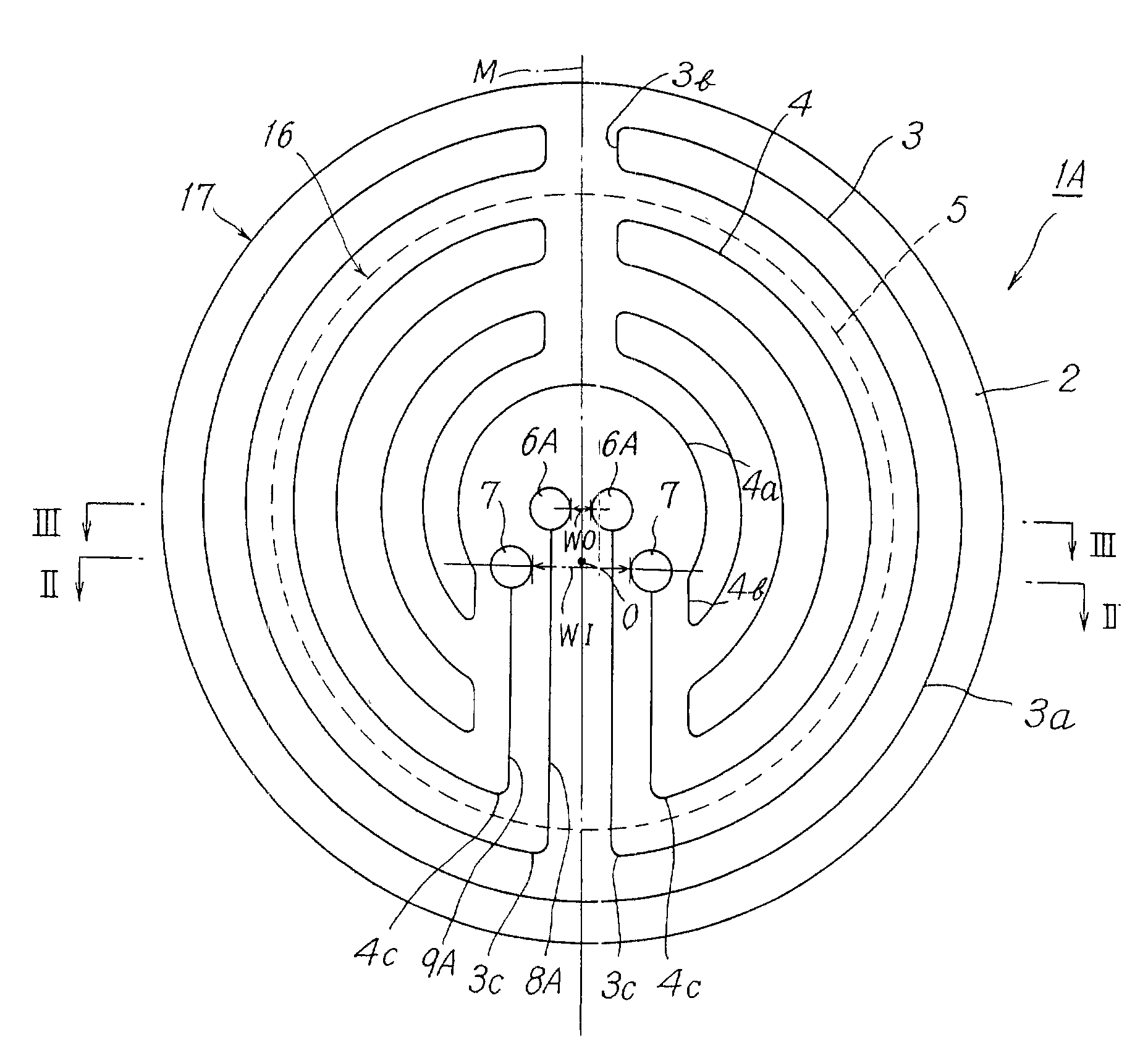
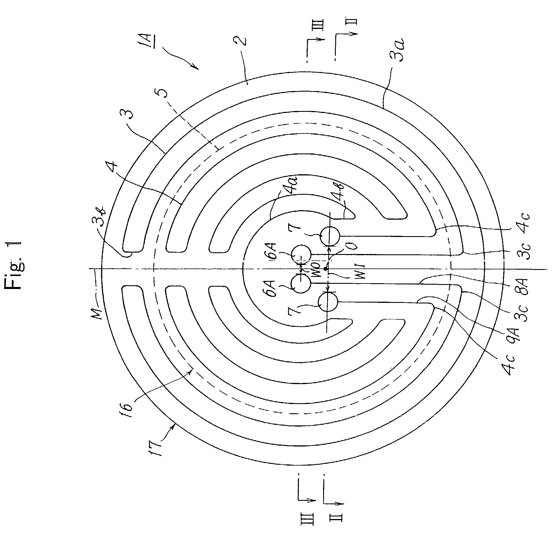
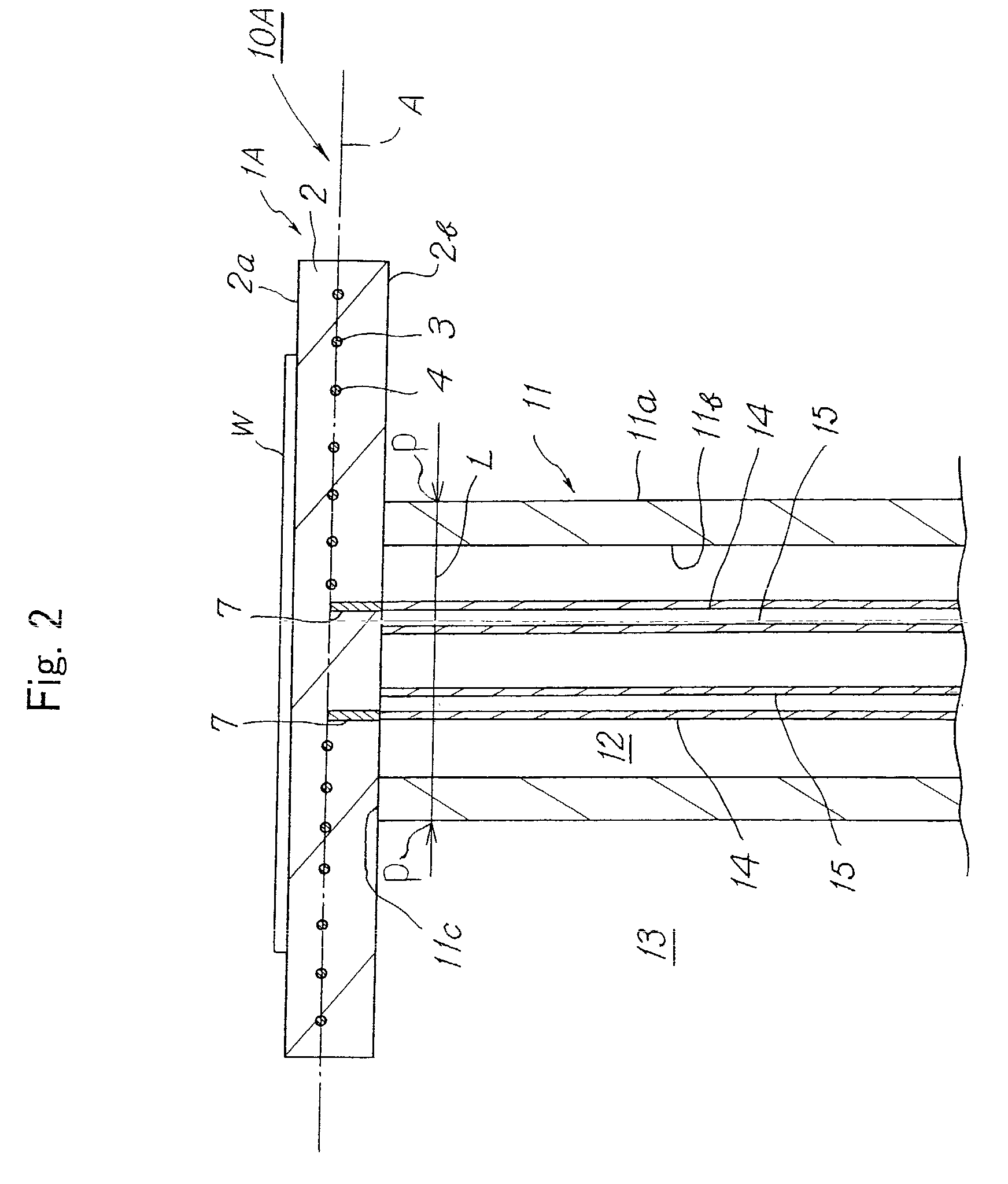
[0070]The heating apparatus shown in FIGS. 1 to 3 was produced. The substrate 2 was made of an aluminum nitride sintered body. The substrate 2 had a diameter φ of 250 mm and a thickness of 10 mm. The second heating element 4 was embedded in the substrate 2 and in the inner zone 16 having a diameter φ of 200 mm, which corresponded with the diameter of a semiconductor wafer to be mounted on the mounting face. The first heating element 3 was embedded in the substrate 2 and in the outer zone 17 whose inner diameter was 200 mm and outer diameter was 250 mm. Each of the heating elements had a shape of a coil spring and was made of molybdenum. Each of the terminals 6A and 7 had a cylindrical shape and was made of molybdenum. The conductive connectors 8A and 9A were molybdenum wires.

[0071]The supporting member 11 was formed of an aluminum nitride sintered body. The supporting member 11 had an outer diameter φ of 80 mm, an inner diameter φ of 50 mm and a length of 250 mm. The supporting memb...

example 2

[0072]The heating apparatus 10B shown in FIGS. 4 to 6 was produced. The substrate 2 was formed of an aluminum nitride sintered body. The substrate 2 had a diameter φ of 250 mm and a thickness of 10 mm. The second heating element 4 was embedded in the substrate and in the inner zone 16 having a diameter φ of 200 mm, which corresponded with the diameter of a semiconductor wafer to be mounted on the mounting face. The first heating element 3 was embedded in the substrate 2 and in the outer zone 17 whose inner diameter was 200 mm and outer diameter was 250 mm. Each of the heating elements had a shape of a coil spring and was made of molybdenum. Each of the terminals 6B and 7 had a cylindrical shape and was made of molybdenum. The conductive connectors 9A and 8B were molybdenum wires. The connecting member 15 is formed of a coil spring made of molybdenum.

[0073]The supporting member 11 same as the example 1 was prepared. The supporting member 11 was solid-phase welded to the back face 2b ...


PUM


Abstract

A heating apparatus for a semiconductor producing system is provided, including a heater having a mounting face, an opposed back face, a first resistance heating element, a second resistance heating element provided along substantially the same plane as the first heating element, a first terminal connected with the first heating element and a second terminal connected with the second heating element. A supporting member is fixed to the back face of the heater. First and second power supply means are respectively connected with the first and second terminals and contained in an inner space of the supporting member. A conductive connector connects the first heating element and the first terminal but not the second heating element. The first heating element is provided in a first zone, the second heating element is provided in a second zone, and the conductive connector is provided in the plane and the second zone.

Description

[0001]This application claims the benefit of Japanese Patent Application P2001-326479 filed on Oct. 24, 2001, the entirety of which is incorporated by reference.BACKGROUND OF THE INVENTION[0002]1. Field of the Invention[0003]The invention relates to a heating apparatus.[0004]2. Related Art Statement[0005]In a system for producing semiconductors, a ceramic heater may be provided for heating a wafer so as to deposit a semiconductor thin film on the wafer from gaseous raw materials such as silane gas by means of thermal CVD or the like. So called two-zone heaters are known as such ceramic heater. Such a two-zone heater has a ceramic substrate and inner and outer resistance heat generators embedded within the substrate. Separate power supply terminals are connected to the respective heat generators so that electric power may be applied independently on the respective generators. The inner and outer heat generators may be thus independently controlled.[0006]Examples of such two-zone heat...

Claims


Application Information

Patent Timeline
Patent Type & Authority Patents(United States)
IPC IPC(8): H05B3/68H05B3/50H05B3/00H01L21/00H01L21/02H01L21/20H01L21/205H05B3/02H05B3/03H05B3/06H05B3/10H05B3/14H05B3/18
CPCH01L21/67103H05B3/68H05B3/143H01L21/20
Inventor OKAJIMA, HISAKAZUUNNO, YUTAKAKAWASAKI, KEIJI
Owner NGK INSULATORS LTD
Why Eureka
Try Eureka