Wiring board mounting a capacitor

a capacitor and wiring board technology, applied in the direction of printed circuit non-printed electric components association, sustainable manufacturing/processing, final product manufacturing, etc., can solve the problems of difficult realization of finer wiring, inflexibility in design, and inability to meet the requirements of manufacturing, so as to improve the operational reliability of semiconductor elements and effective decoupling

Active Publication Date: 2007-10-09
SHINKO ELECTRIC IND CO LTD
View PDF11 Cites 83 Cited by
  • Summary
  • Abstract
  • Description
  • Claims
  • Application Information

AI Technical Summary

Benefits of technology

[0014]An object of the present invention is to provide a novel capacitor-mounted wiring board and a method of manufacturing the same in which the equivalent series inductance (ESL) of a mounted capacitor is reduced to allow effective decoupling and, consequently, which can contribute to an improvement in the operational reliability of a semiconductor element or the like to be mounted.
[0016]According to the constitution of the capacitor-mounted wiring board of the present invention, since the capacitor and the wiring layer for power supply (or ground) are placed close to each other, the magnetic coupling between the current flowing through the capacitor and the current flowing through the relevant wiring layer is enhanced. Further, since the directions of the currents thereof are reversed to each other, magnetic fields generated by the currents cancel each other. As a result, the equivalent series inductance (ESL) of the capacitor decreases in appearance under the influence of the magnetic field (magnetic field acting in a direction in which the magnetic field generated by the capacitor is canceled) originating from the relevant wiring layer. Namely, the ESL of the capacitor can be reduced. This makes it possible to perform effective decoupling and can contribute to an improvement in the operational reliability of a semiconductor element or the like to be mounted.
[0017]In this case, by further reducing the distance between the capacitor and the relevant wiring layer, the distribution of the current flowing through the capacitor can be concentrated in the vicinity of the relevant wiring layer, which is a target of magnetic coupling. Accordingly, the ESL can be more effectively reduced.

Problems solved by technology

However, since conventional printed wiring boards have needed large areas for the formation of via holes, flexibility in design has been limited, and finer wiring has been difficult to realize.
However, on the other hand, since wiring patterns are close to each other in such a multilayer wiring board (semiconductor package), problems can occur, such as an occurrence of crosstalk noise between the wiring patterns, a fluctuation in the potential of a power supply line or a ground line, and the like.
In particular, in a semiconductor package in which a semiconductor element, an electronic component, or the like, required to perform a high-speed switching operation, is mounted, the tendency of crosstalk noise to occur increases as the frequency increases.
Further, switching noise occurs due to a switching element turning on and off at high speed, and this makes the potentials of a power supply line and the like ready to fluctuate.
This leads to a deterioration in the operational reliability of the mounted semiconductor element or the like, and therefore is not preferable.
Further, the routing length of interconnections connecting the capacitor and the semiconductor element increases, and this may cause an increase in inductance.
Namely, there has been a problem in that the ESL of the capacitor cannot be necessarily sufficiently reduced depending on the relationship between the placement of the capacitor and that of a wiring pattern in the vicinity thereof and the relationship between the directions of currents flowing therethrough.

Method used


Image

  • Wiring board mounting a capacitor
  • Wiring board mounting a capacitor
  • Wiring board mounting a capacitor

Examples


first embodiment

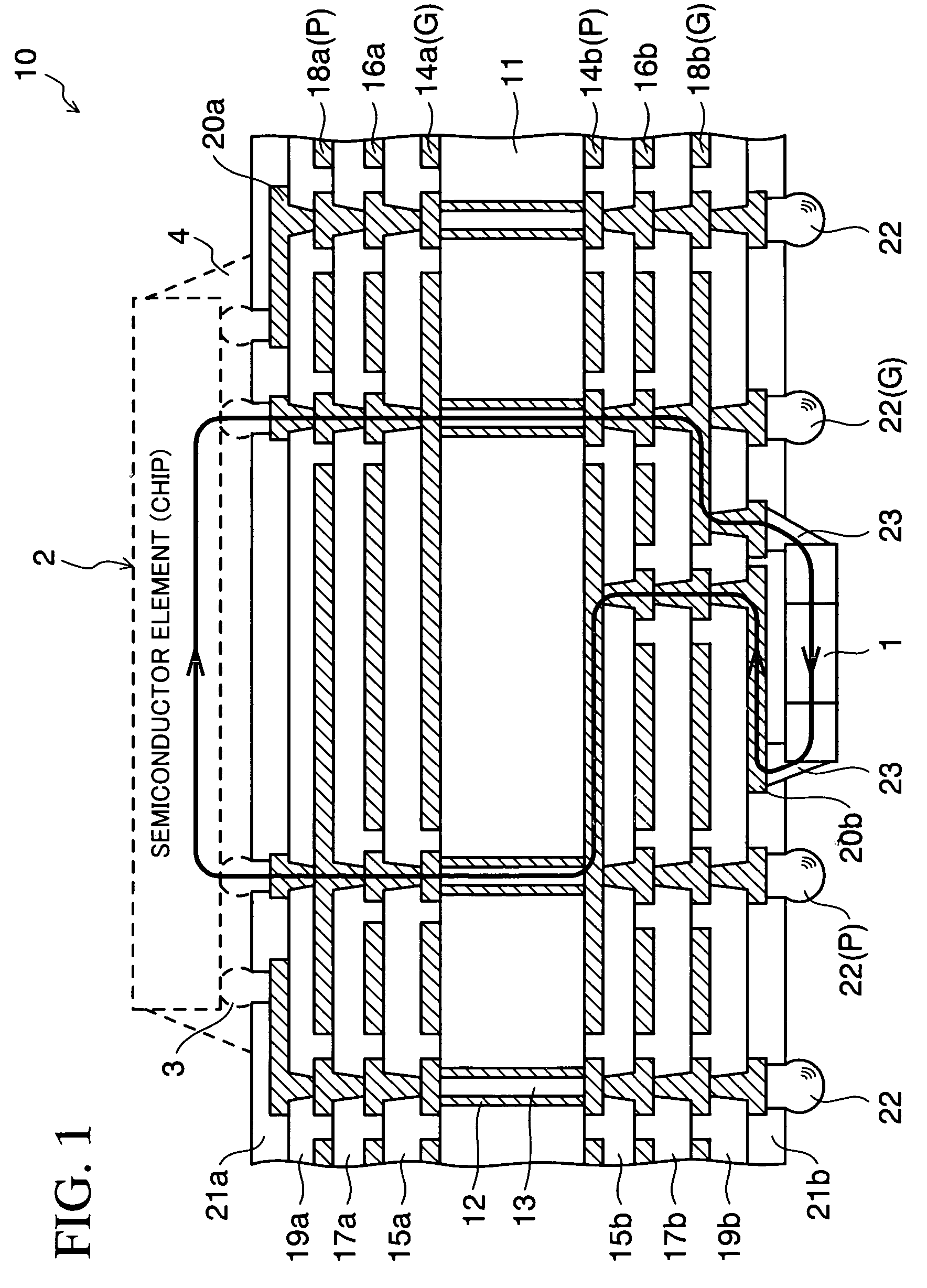
[0033]FIG. 1 schematically shows, in a cross-sectional view, a constitution of a capacitor-mounted wiring board (semiconductor package) according to the present invention. In the illustrated example, there is shown a constitution for the case where a chip capacitor 1 is surface-mounted on the back surface (opposite surface to the surface on which a semiconductor element 2 is to be mounted) of the semiconductor package 10.

[0034]In the semiconductor package 10 according to this embodiment, reference numeral 11 denotes an insulating base material (e.g., a glass cloth immersed in thermosetting resin, such as epoxy resin or polyimide resin) as a core substrate of this package; reference numeral 12 denotes a conductor (e.g., metal such as copper (Cu)) formed on the inner wall of a through hole which is formed at a required position in the core substrate 11 to pierce the core substrate 11 in the thickness direction; reference numeral 13 denotes an insulator (e.g., epoxy resin) filled in th...

second embodiment

[0042]FIG. 2 schematically shows, in a cross-sectional view, a constitution of a capacitor-mounted wiring board (semiconductor package) according to the present invention.

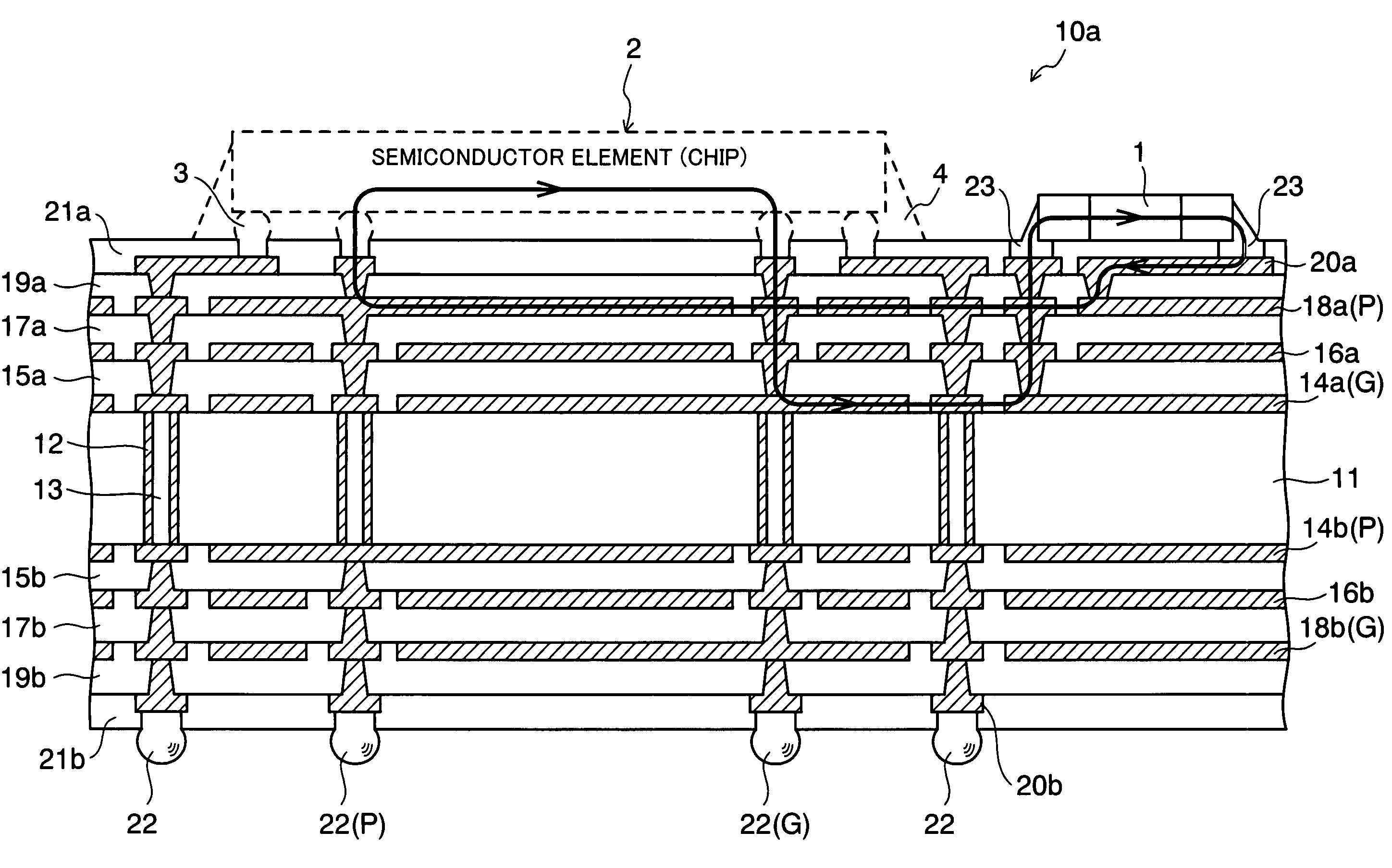
[0043]The semiconductor package 10a according to this embodiment differs from the semiconductor package 10 (FIG. 1) according to the aforementioned first embodiment, in that the chip capacitor 1 is surface-mounted in a region (right side in the illustrated example) around a semiconductor element mount region on the top surface (the same surface as the surface on which the semiconductor element 2 is to be mounted) of this package 10a. Other constitutions and the functions thereof are basically the same as those in the case of the first embodiment, and thus the explanation thereof is omitted.

[0044]According to this second embodiment, electrical characteristics for the entire semiconductor device (semiconductor package 10a in a state of having the semiconductor element 2 mounted thereon) can be further improved compar...

third embodiment

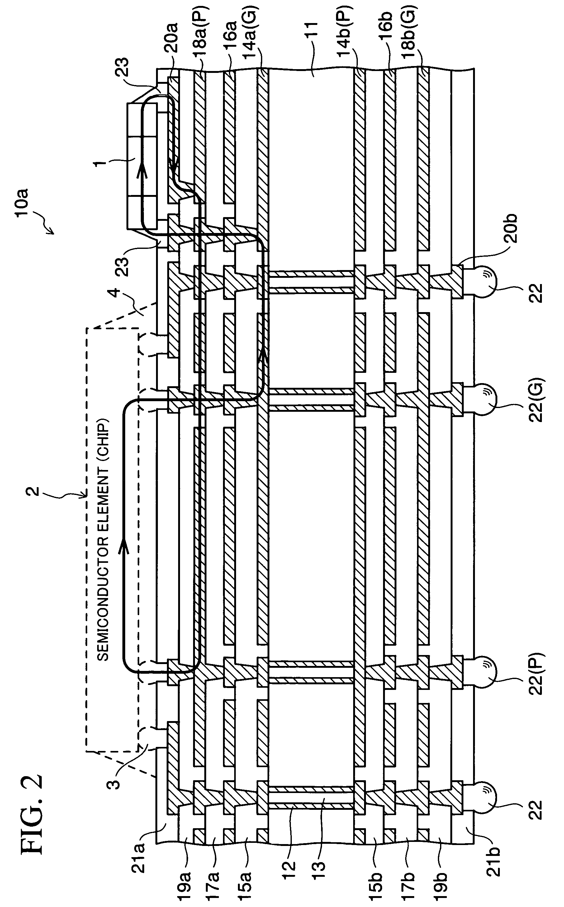
[0045]FIG. 3 schematically shows, in a cross-sectional view, a constitution of a capacitor-mounted wiring board (semiconductor package) according to the present invention.

[0046]The semiconductor package 10b according to this embodiment differs from the semiconductor package 10a (FIG. 2) according to the aforementioned second embodiment, in that a ground plane (i.e., a ground wiring layer 18a having a current flowing therethrough to generate a magnetic field in a direction in which the magnetic field generated by the current flowing through the capacitor 1 is canceled) is placed directly under the chip capacitor 1. This difference in arrangement reduces the number (length) of layers of via holes existing in the path of the current flowing through the capacitor 1 compared with the case of the second embodiment, and decreases inductance generated in the path of the current flowing through the capacitor. Accordingly, electrical characteristics for the entire semiconductor device (semico...


PUM


Abstract

In a capacitor-mounted wiring board, a plurality of wiring layers each patterned in a required shape are stacked with insulating layers interposed therebetween and are connected to each other via conductors formed to pierce the insulating layers in the direction of thickness. A decoupling capacitor is electrically connected to a wiring layer used as a power supply line or a ground line in the vicinity of the wiring layer, and mounted such that, when a current is passed through the capacitor, the direction of the current is reversed to that of the current flowing through the relevant wiring layer.

Description

CROSS-REFERENCE TO RELATED APPLICATIONS[0001]This application is based on and claims priority of Japanese Patent Application No. 2004-104660 filed on Mar. 31, 2004, the entire contents of which are incorporated herein by reference.BACKGROUND OF THE INVENTION[0002](a) Field of the Invention[0003]The present invention relates to a wiring board in which a capacitor is mounted. More particularly, the present invention relates to a novel structure of a wiring board in which a decoupling capacitor is mounted, for mounting a semiconductor element (chip), an electronic component, or the like, required to perform a high-speed switching operation, and to a method of manufacturing the same.[0004]In this specification, for convenience, a wiring board is also referred to as a “semiconductor package” in the sense that it plays a role as a package on which a semiconductor element or the like is mounted. Further, a wiring board (semiconductor package) in a state of having a semiconductor element or...

Claims


Application Information

Patent Timeline
Patent Type & Authority Patents(United States)
IPC IPC(8): H01L29/00H05K1/03H05K1/14H05K3/46H01L21/4763H01L23/12H01L23/498H01L23/50H01L25/00H05K1/02H05K1/11H05K1/18
CPCH01L23/49822H05K1/0231H01L23/50H01L2224/16235H01L2224/16H01L2924/01004H01L2924/01078H01L2924/01079H01L2924/15192H01L2924/15311H01L2924/19105H01L2924/19106H05K1/113H05K1/185H05K3/4602H05K2201/0792H05K2201/09772H05K2201/10636H01L2224/73204Y02P70/50B60Q1/441B60Q1/444B60Q1/525B60Y2400/301
Inventor SUNOHARA, MASAHIROMURAYAMA, KEIHIGASHI, MITSUTOSHIGOMYO, TOSHIOTAKEUCHI, YUKIHARU
Owner SHINKO ELECTRIC IND CO LTD
Why Eureka
Try Eureka