Display device

Inactive Publication Date: 2007-10-09
SEMICON ENERGY LAB CO LTD
View PDF26 Cites 17 Cited by
  • Summary
  • Abstract
  • Description
  • Claims
  • Application Information

AI Technical Summary

Benefits of technology

[0019]In the light of the foregoing, the present invention was made in order to solve the above-mentioned problems inherent in the prior art, and it is therefore an object of the present invention to provide a display device which is capable of reducing the influence which is exerted on the image display by the noises generated in the drive circuit (in particular, in the shift register circuit).

Problems solved by technology

In this connection, the noise which has become conventionally a problem is one of the factors which exert the bad influence on the characteristics to dominate the display characteristics and the electromagnetic radiation.
As described above, the noises which are generated by inputting at least one pair of signals in which the signal rise time period (tr) and the signal fall time period (tf) are finely different from each other to the drive circuit exert the bad influence on the display characteristics and the electromagnetic radiation, and hence the problem as will hereinbelow be described arises particularly in the case where the signal having the high frequency band is employed.
Those noises exert the bad influence on the video signal when displaying the image on the screen so that the level of the electromagnetic radiation is varied and hence it is difficult to control the level of the electromagnetic radiation within the EMC Standards.
In addition, there is the possibility that the sharp noises each having the large amplitude exert the bad influence on other circuits as well.
As described above, there arises the problem that the noises each having a sharp waveform which have been generated in the shift register circuit or the like are superimposed on the video signal so that the voltage applied to pixel electrodes is varied to change the display.
However, the circuit configuration becomes complicated in which on the basis of the above-mentioned method, the ideal clock waveforms are formed, and the phase difference between one pair of signals is made just zero, and hence it is difficult to design the circuit.
In particular, with respect to one pair of signals of high frequency, it is difficult to make one signal aligned with the other signal, and also it is very difficult to make one signal aligned with the other signal.

Method used


Image

  • Display device
  • Display device
  • Display device

Examples


embodiment 1

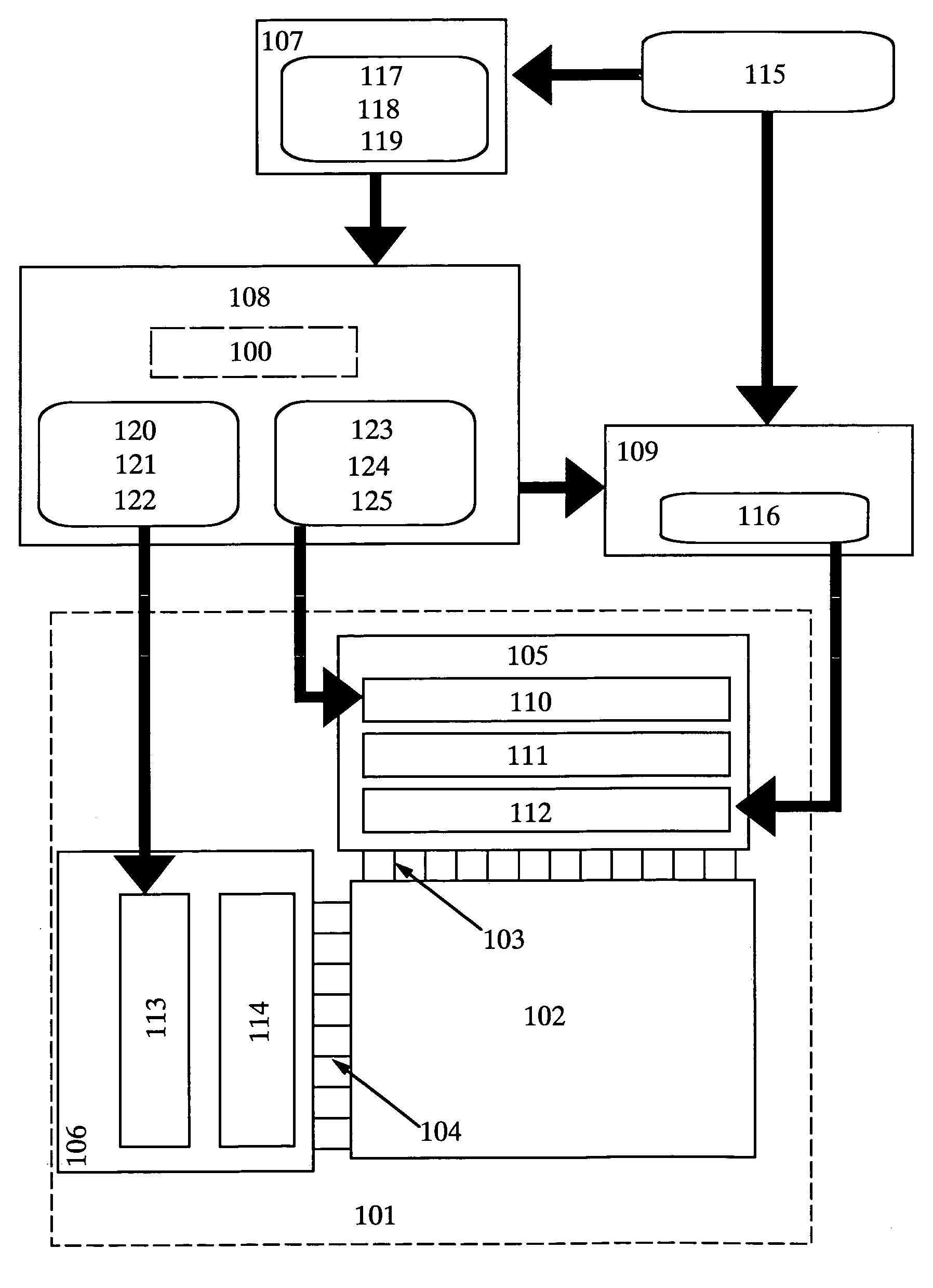
[0050]FIG. 1 is a schematic block diagram showing a configuration of an embodiment 1 of a liquid crystal display device according to the present invention. The liquid crystal display device shown in FIG. 1 is mainly constituted by a liquid crystal panel 101, a signal producing unit 107, a video signal processing circuit 109, and a control circuit 108.

[0051]In this connection, the signal producing unit 107, the video signal processing circuit 109, the control circuit 108 and the like are, for example, mounted on another printed substrate which is connected to the liquid crystal panel 101 through cables, a flexible wiring board and the like. In addition, it is needless to say that it is preferable that a part of or all of the signal producing unit 107, the video signal processing circuit 109, the control circuit 108 and the like is or are provided on the same substrate as that of the liquid crystal panel 101, since the integration can be realized.

[0052]The liquid crystal panel 101 is ...

embodiment 2

[0071]While in the embodiment 1, there has been adopted the method wherein a plurality of signals the phases of which are intentionally shifted from each other are inputted to the drive circuit in order to prevent the noises from being superimposed on each other, in the present embodiment, an example of another configuration is adopted.

[0072]In the present embodiment, one pair of signals the phases of which are intentionally shifted from each other in a similar manner to that of the embodiment 1 are inputted to the drive circuit. Then, the signals the phases of which are shifted from each other are adjusted in phases in the inside of the drive circuit to cancel out any of the noises to output the signals which are aligned with each other. By adopting such a configuration, the video signal which is free from any of noises can be formed and also the excellent display characteristics can be obtained.

embodiment 3

[0073]FIG. 4 is a schematic view showing the outline of a projection type image display device (a rear projector) employing a three-plates optical system. In the projector of the present embodiment, the projected light which has been projected from a light source 401 is separated into the primaries R, G and B which are in turn respectively introduced into three-sheets of TFT liquid crystal panels 400 for displaying thereon the images having the respective colors through mirrors 404. Then, the light beams which have been obtained on the basis of the modulation in the respective TFT liquid crystal panels are combined with each other through an optical system 406 to be a video light beam which is in turn applied to the screen so that the color image is projected.

[0074]When by employing the liquid crystal panel, the signal processing circuit and the control circuit shown in the above-mentioned embodiment 1, the input image signals are supplied to the respective liquid crystal panels, th...


PUM


Abstract

An image display device in which a positive clock signal and a negative clock signal of high frequency are made slightly different in a pulse rise time (tr) and a pulse fall time (tf) from each other to reduce the magnitude of noises each having a sharp waveform which noises are generated in a drive circuit (in particular, a shift register circuit) by being superimposed on each other, thereby providing the image display which has the high picture quality and the high definition and which is free from the turbulence of the image. Delay means is provided in a signal producing unit, a control unit, or an input wiring distributed to the associated circuit in order to shift the phases of the positive clock signal and the negative clock signal from each other by the pulse fall time period (tf), thereby reducing the influence exerted on the display.

Description

BACKGROUND OF THE INVENTION[0001]1. Field of the Invention[0002]The present invention relates in general to an active matrix type display device which employs a display material such as liquid crystal and which self-contains a drive circuit, and more particularly to the technology of relaxing the bad influence which is exerted on the display by the noises generated in the drive circuit or the like to control the unnecessary radiated level within the various EMC (Electromagnetic Compatibility) regulations.[0003]2. Description of the Related Art[0004]In recent years, the technology of forming thin film transistors (hereinafter, referred to as “TFTs” for short, when applicable) on an inexpensive glass substrate has made rapid development. This reason is that the demand for active matrix type liquid crystal display devices has been increased.[0005]The active matrix type liquid crystal display device is such that the TFTs are arranged so as to individually correspond in position to sever...

Claims


Application Information

Patent Timeline
IPC IPC(8): G09G3/36G02F1/13G02F1/133G09G3/20
CPCG09G3/3688G09G2330/06G02F1/133
Inventor HIROKI, MASAAKI
Owner SEMICON ENERGY LAB CO LTD
Why Eureka
Try Eureka