Non-volatile semiconductor memory device allowing concurrent data writing and data reading

a non-volatile, memory device technology, applied in the direction of information storage, static storage, digital storage, etc., can solve the problems of limited memory cell current, insufficient read current supply, and inability to read fast data, etc., to reduce accessing time

Inactive Publication Date: 2007-10-23
RENESAS ELECTRONICS CORP
View PDF10 Cites 111 Cited by
  • Summary
  • Abstract
  • Description
  • Claims
  • Application Information

AI Technical Summary

Benefits of technology

[0014]An object of the present invention is to provide a non-volatile semiconductor memory device that can reduce an accessing time.
[0015]Another object of the present invention is to provide a non-volatile semiconductor memory device that can implement an operation mode similar to that in another memory device such as a dynamic random access memory (DRAM).
[0016]A specific object of the present invention is to provide a non-volatile semiconductor memory device having a variable resistance element type memory cell structure, which can reduce an accessing time without increasing the current consumption.
[0020]In the non-volatile semiconductor memory device according to the first aspect, a precharge circuit and an amplifier circuit are arranged for each bit line, and a memory cell current is not required to directly drive an internal data line. The capacitance driven by the memory cell current flowing through a selected memory cell can be reduced, and internal data reading can be performed at high speed. Accordingly, a read accessing time can be reduced.
[0021]In the non-volatile semiconductor memory device according to the second aspect, a write circuit performing data writing and a read circuit performing data reading are made operable concurrently. Thus, data writing and data reading can be performed in parallel. Two instructions of writing and reading can be executed concurrently, and a memory system achieving fast processing can be structured. Additionally, operation modes such as read-modify-write and write-verify can be implemented, and improvement in performance and reduction in write time can be achieved.

Problems solved by technology

However, when a source line is provided commonly to a plurality of read blocks and the interconnection resistance of the source line is large, such a problem occurs that a read current (memory cell current) from a selected memory cell (TMR element) flows to raise the source line potential (in data reading, the source line is coupled to the ground potential), the read current cannot be sufficiently supplied, and fast data reading cannot be achieved.
Further, due to the raised source line potential, the memory cell current may be limited and correct data reading may not be performed.
However, with such a configuration, it is still inadequate to obtain a correct read current, due to the interconnection resistance and the distribution of the source potential (floating-up) over the entire source line as the source line is arranged extending along a plurality of read blocks and thus the interconnection length is large.
Thus, it is allowed to alternatively perform data writing and data reading, and it is not allowed to implement an operation mode performing writing and reading in parallel, such as read-modify-write mode in which write data is changed by read data.
Accordingly, there are problems that the load of the internal data line is large, the read current cannot be driven fast in data reading, and fast accessing cannot be achieved.
Therefore, there is a problem that fast reading cannot be achieved.

Method used


Image

  • Non-volatile semiconductor memory device allowing concurrent data writing and data reading
  • Non-volatile semiconductor memory device allowing concurrent data writing and data reading
  • Non-volatile semiconductor memory device allowing concurrent data writing and data reading

Examples


first embodiment

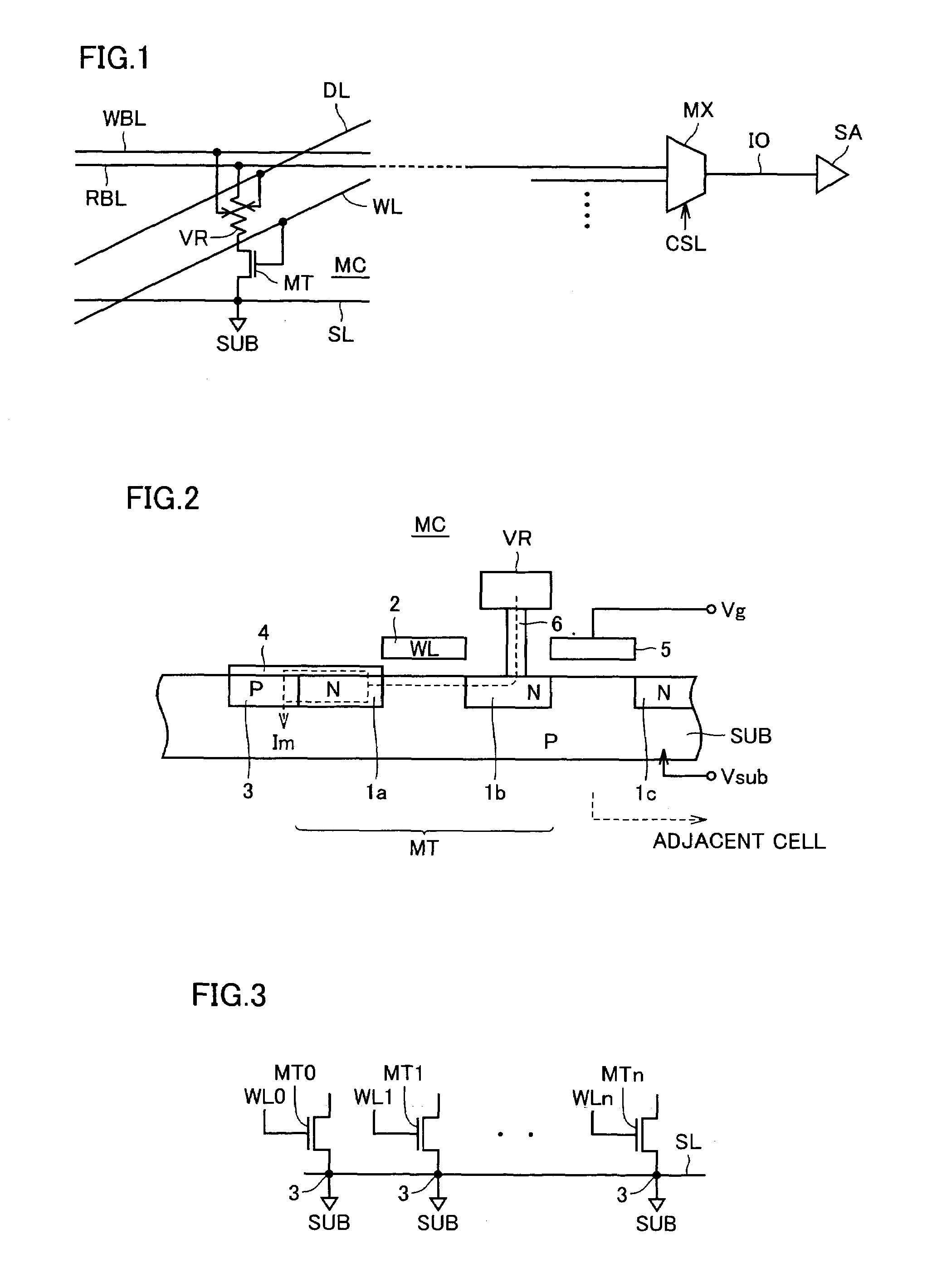
[0052]FIG. 1 schematically shows a configuration of a portion related to one memory cell of a non-volatile semiconductor memory device according to a first embodiment of the present invention. A memory cell MC is arranged corresponding to an intersection of a digit line DL as well as a word line WL and a write bit line WBL as well as a read bit line RBL. In the first embodiment, write bit line WBL for supplying a write current in data writing to memory cell MC, and read bit line RBL for supplying a read current to memory cell MC in data reading are separately provided.

[0053]Write bit line WBL and read bit line RBL are arranged in parallel, and word line WL and digit line DL are arranged in parallel.

[0054]Memory cell MC includes a variable resistance element VR having its resistance value set in accordance with storage information, and a select transistor MT for coupling variable resistance element VR to source line SL in accordance with a signal on word line WL. Variable resistance ...

second embodiment

[0094]FIG. 10 schematically shows a configuration of a memory cell of a non-volatile semiconductor memory device according to a second embodiment of the present invention. In FIG. 10, a memory cell MC includes a variable resistance element VRP formed of a phase change element changing its crystal state in accordance with storage data, select transistors TRa and TRb connected in parallel between variable resistance element VRP and source line SL. To the gates of select transistors TRa and TRb, word lines WL are connected, and word lines WL are supplied with the same select signal. Similarly to the first embodiment, source line SL is electrically coupled to substrate region SUB through an impurity region.

[0095]Variable resistance element VRP is connected to bit line BL. Variable resistance element VRP is formed of, for example, a GST (Ge—Sb—Te) film, and its crystal state changes between a crystalline state and an amorphous state in accordance with storage data. In the crystalline sta...

third embodiment

[0110]FIG. 14 schematically shows a configuration of a main portion of a non-volatile semiconductor memory device according to a third embodiment of the present invention. In FIG. 14, memory cells MC equivalently arranged in three rows and three columns are representatively shown. In the arrangement of memory cells MC shown in FIG. 14, to memory cells MC aligned in column direction (X direction), a read bit line and a source line SL are arranged in pair. Specifically, a pair of read bit line RBL1 and source line SL1 are arranged extending along X direction, and a pair of read bit line RBL2 and source line SL2 are arranged extending in X direction. Similarly, read bit lines RBL3 and source lines SL3 are arranged extending along X direction.

[0111]In the array of memory cells MC, the memory cells aligned in Y direction are coupled to different word and digit lines. In FIG. 14, word lines WL1-WL7 and digit lines DL1-DL7 are shown.

[0112]Memory cell MC includes a variable resistance eleme...


PUM


Abstract

A write bit line and a read bit line are provided separately for a memory cell. A source line connecting to the memory cell is formed of a source impurity region the same in conductivity type as a substrate region. A memory cell transistor and the source impurity region are connected by a metal interconnection line of a low resistance. A rise in the source line potential can be prevented, and a memory cell current can reliably be generated according to storage data. Further, fast data reading can be achieved. Additionally, by performing precharging and data amplification in a unit of read bit line, the load of the read bit line can be alleviated to achieve fast reading. An accessing time of a non-volatile semiconductor memory device that uses a variable resistance element as a storage element is reduced without increasing the current consumption.

Description

BACKGROUND OF THE INVENTION[0001]1. Field of the Invention[0002]The present invention relates to a non-volatile semiconductor memory device, and particularly, to a configuration for reducing a time required for data writing / reading in a non-volatile semiconductor memory device. Specifically, the present invention relates to an array configuration for and an accessing scheme for fast accessing of a non-volatile semiconductor memory device containing a variable resistance element, such as a magneto-resistance element or a phase change element, as a storage element.[0003]2. Description of the Background Art[0004]Among semiconductor memory devices that store data in a non-volatile manner, there is included a magnetic semiconductor memory device (MRAM: Magnetic Random Access Memory) that utilizes a tunnel junction (MTJ: Magnetic Tunnel Junction) structure exhibiting a tunneling magneto-resistance (TMR) effect as a storage element.[0005]In a TMR element (or an MTJ element), a storage elem...

Claims


Application Information

Patent Timeline
Patent Type & Authority Patents(United States)
IPC IPC(8): G11C11/00
CPCG11C11/16G11C13/0004G11C13/0061G11C13/0069G11C13/004G11C2013/0076
Inventor OOISHI, TSUKASA
Owner RENESAS ELECTRONICS CORP
Why Eureka
Try Eureka