Pulsed deposition layer gap fill with expansion material

a nanolaminate and expansion material technology, applied in the field of dielectric gap filling, can solve problems such as seam and void formation, achieve the effects of reducing the incidence of voids or weak spots, eliminating seams and voids, and improving the gap-fill performance of doped materials

Active Publication Date: 2007-10-30
NOVELLUS SYSTEMS
View PDF58 Cites 47 Cited by
  • Summary
  • Abstract
  • Description
  • Claims
  • Application Information

AI Technical Summary

Benefits of technology

[0006]The present invention addresses this need by providing conformal dielectric deposition (e.g., pulsed deposition layer (PDL) processing or ALD) processes supplemented with a deposited expansion material that can fill high aspect ratio (at least 3:1, typically at least 5:1, for example 7:1 or greater), narrow width (typically sub 0.13 micron, for example 0.1 micron or less) gaps with significantly reduced incidence of voids or weak spots. The invention relates to a deposition technique for improving the gap-fill performance of doped or un-doped silica glass in IMD/ILD, PMD, and STI gap fill applications. Both conformal (PDL or ALD) and line

Problems solved by technology

Both conformal (PDL or ALD) and line of sight deposition processes result in the forma

Method used


Image

  • Pulsed deposition layer gap fill with expansion material
  • Pulsed deposition layer gap fill with expansion material
  • Pulsed deposition layer gap fill with expansion material

Examples


example

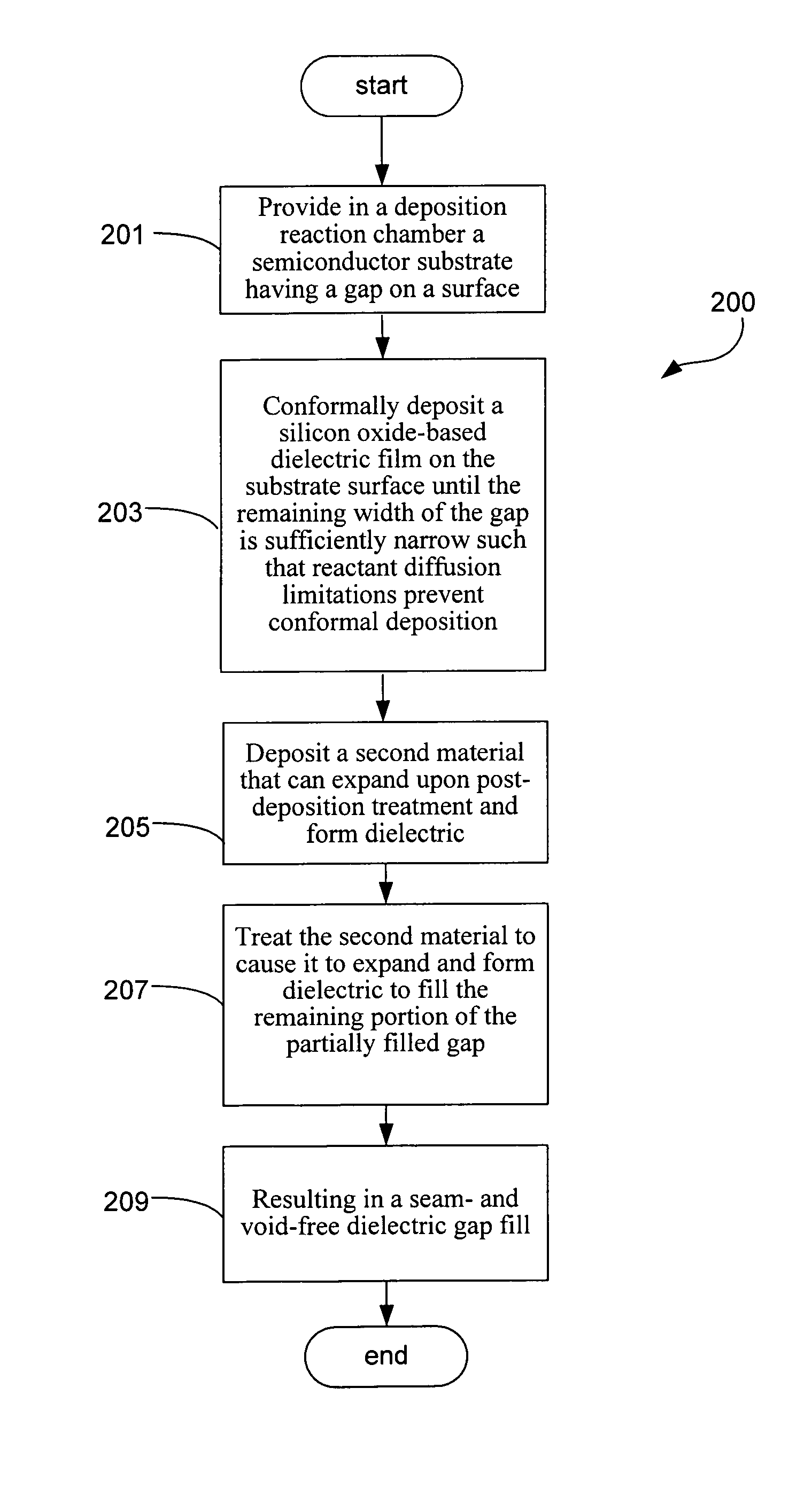
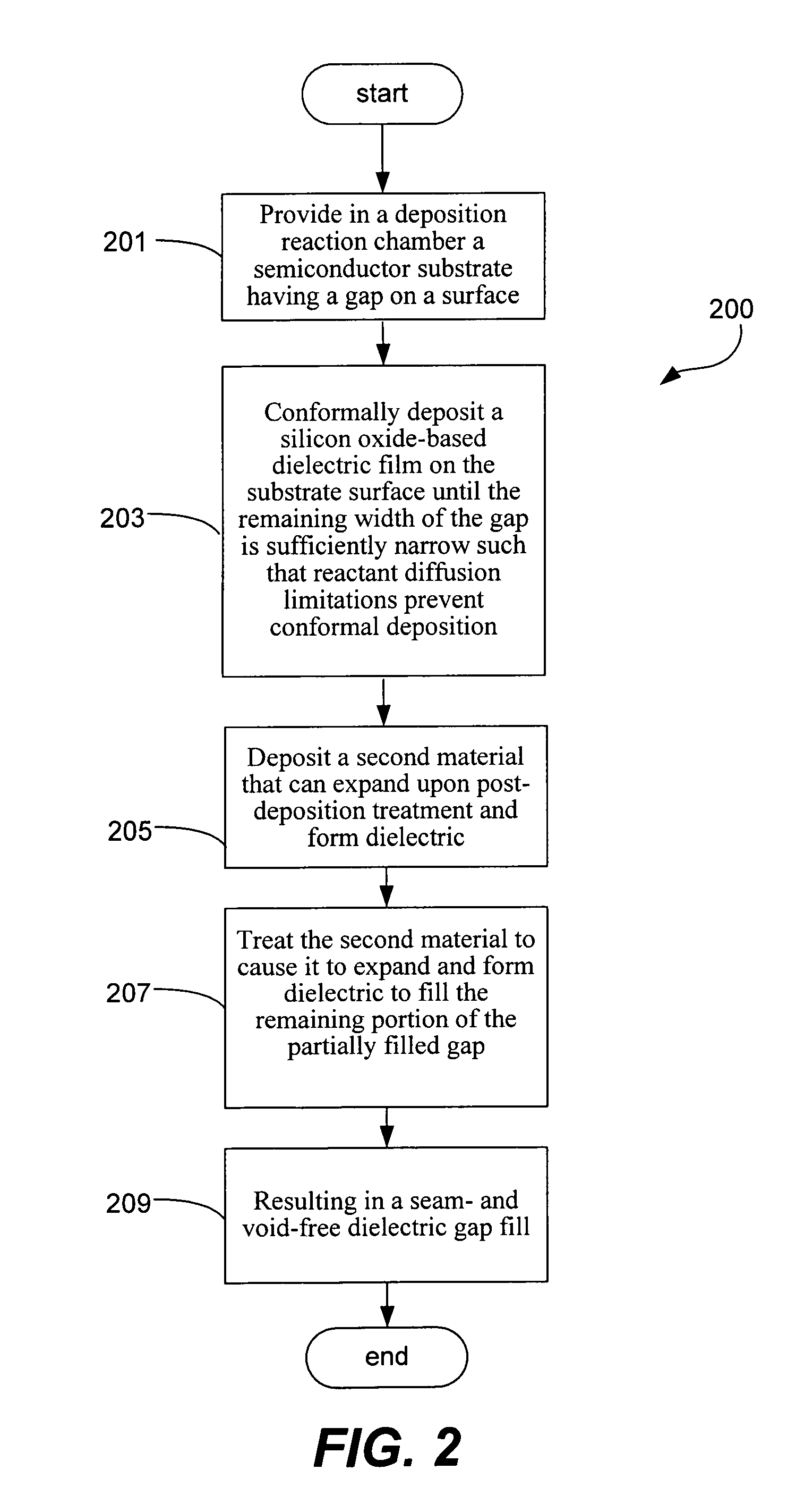
[0055]The following example provides details relating to the practice and advantages of a gap fill method in accordance with the present invention. It should be understood the following is representative only, and that the invention is not limited by the detail set forth in this example.

[0056]The feasibility of the method for filling gaps in accordance with the present invention was tested. The following gap fill protocol was used as then samples studied as described below:

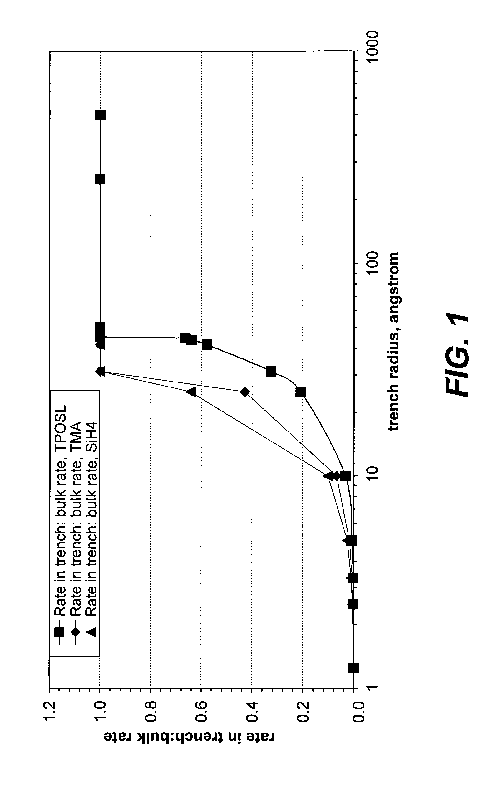
[0057]Gaps smaller than about 75 nm wide with an aspect ratio of greater than 5:1 were partially filled with PDL oxide. PDL gapfill was conducted at 230° C. and 20 Torr, with TPOSL used for silicon oxide precursor, and TMA used to catalyze the reaction of silicon oxide formation, until a gap width of about 200-500 Å, remained unfilled. Polysilicon was deposited in the partially filled gaps by thermal CVD, operating at under 600° C. at subatmospheric pressure with SiH4 as the deposition precursor. All samples were ...


PUM


Abstract

Conformal dielectric deposition processes supplemented with a deposited expansion material can fill high aspect ratio narrow width gaps with significantly reduced incidence of voids or weak spots. The technique can also be used generally to form composites, such as for the densification of any substrate having open spaces or gaps to be filled without the incidence of voids or seams.

Description

BACKGROUND OF THE INVENTION[0001]This invention relates to dielectric gap fill, particularly in high aspect ratio, narrow width recessed features. More specifically, the invention relates to gap fill with a nanolaminate deposition processes enhanced with an expansion material.[0002]It is often necessary in semiconductor processing to fill a high aspect ratio gap with insulating material, for example, for IMD / ILD, PMD, and STI gap fill with doped or un-doped silica glass. As device dimensions shrink and thermal budgets are reduced, void-free filling of high aspect ratio spaces (e.g., AR>3:1) becomes increasingly difficult due to limitations of existing deposition processes. The method currently used for high aspect ratio (AR) gap-fill is deposition of doped or undoped silicon dioxide assisted by high density plasma chemical vapor deposition (HDP CVD), a directional (bottom-up) CVD process. Evolving semiconductor device designs and dramatically reduced feature sizes have resulted i...

Claims


Application Information

Patent Timeline
IPC IPC(8): H01L21/762
CPCH01L21/76224H01L21/316H01L21/02107
Inventor PAPASOULIOTIS, GEORGE D.
Owner NOVELLUS SYSTEMS
Why Eureka
Try Eureka