

Electron emitter and light emission element
a technology of light emission element and electron emitter, which is applied in the direction of discharge tube main electrodes, instruments, tubes with screens, etc., can solve the problems of inability to use conventional electron emitters in practical use, inability to accurately measure the emission rate of electrons, and inability to achieve steady emission rate. , to achieve the effect of improving the service life and reliability of the electron emitter and the light emission element for emitting electrons
- Summary
- Abstract
- Description
- Claims
- Application Information
AI Technical Summary
Benefits of technology
Problems solved by technology
Method used
Image

Examples
first embodiment
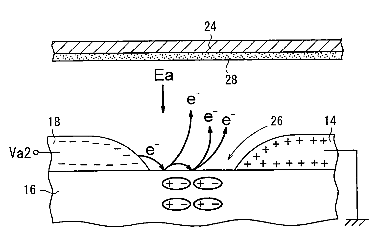
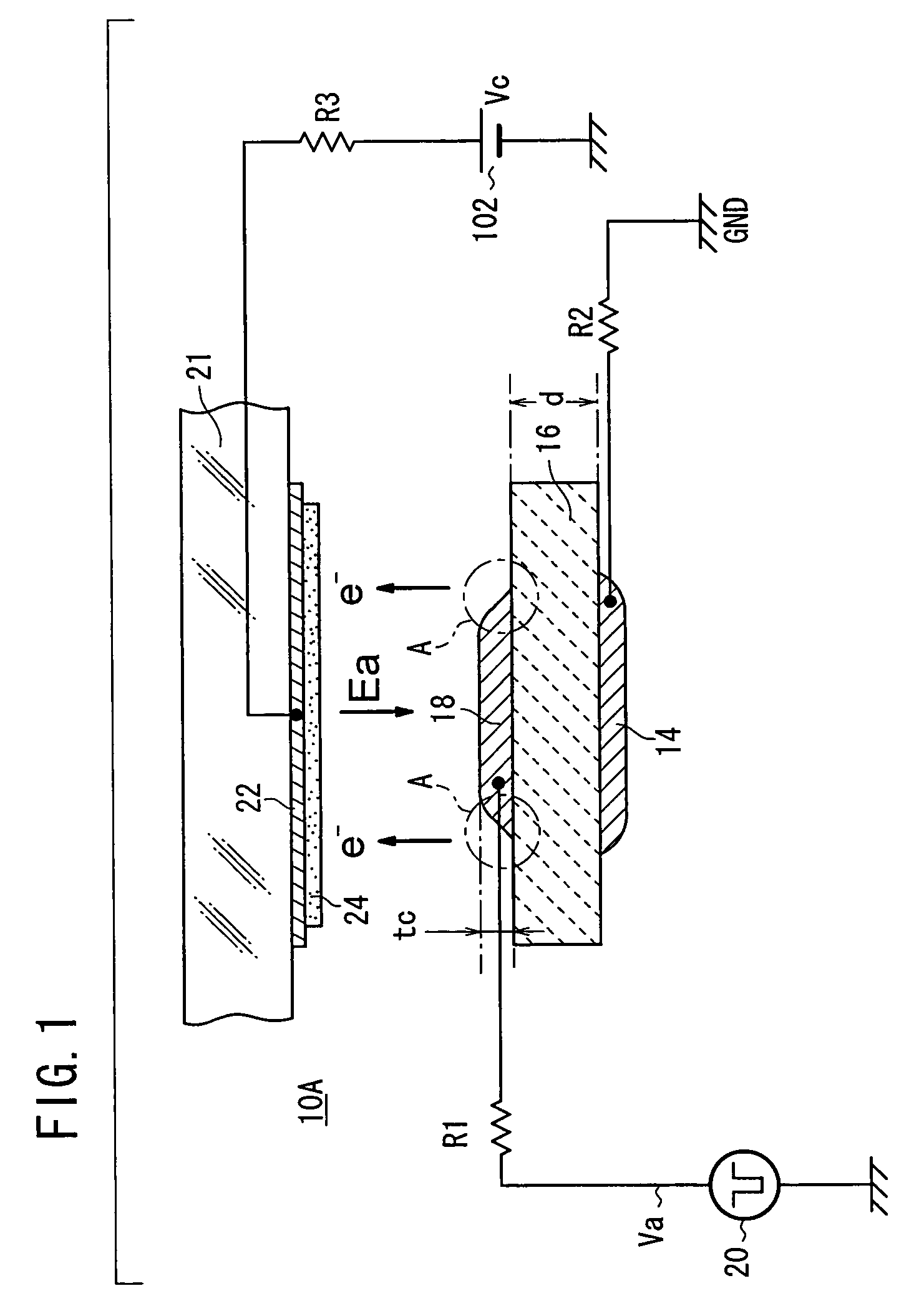
[0046]As shown in FIG. 1, an electron emitter 10A according to the present invention has an emitter section (emitter element) 16 having a plate shape, a first electrode (a cathode electrode) 18 formed on a front surface of the emitter section 16, and a second electrode (an anode electrode) 14 formed on a back surface of the emitter section 16.
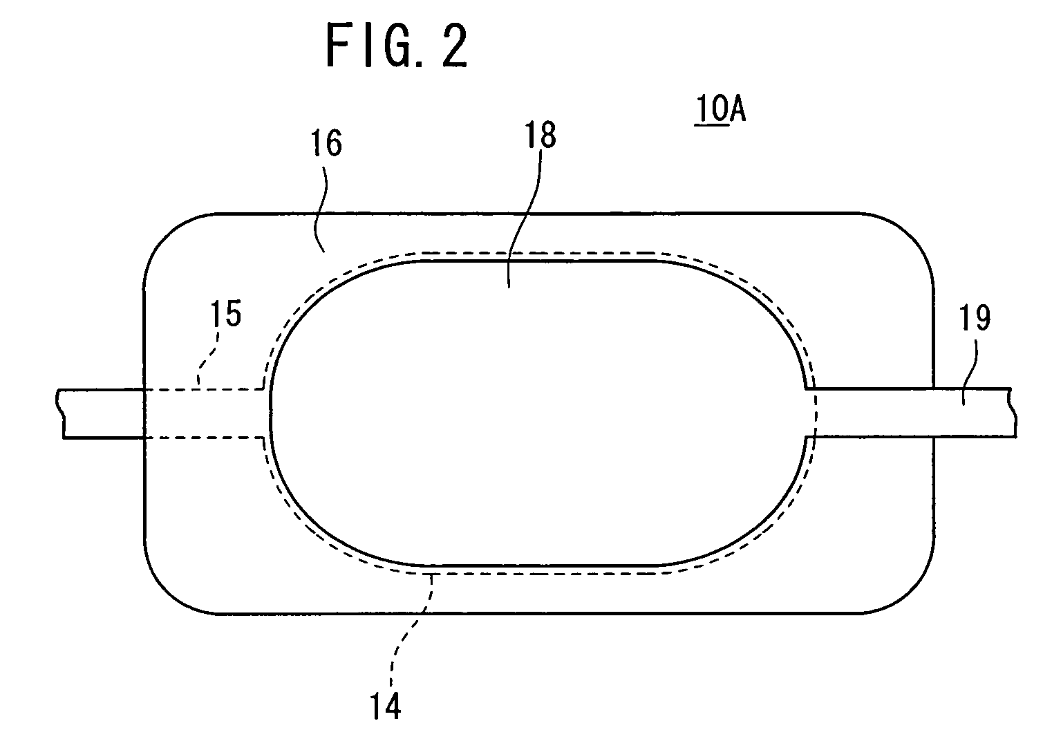
[0047]A drive voltage Va from a pulse generation source 20 is applied between the cathode electrode 18 and the anode electrode 14 through a resistor R1. In an example shown in FIG. 1, the anode electrode 14 is connected to GND (ground) and hence set to a zero potential. However, the anode electrode 14 may be set to a potential other than the zero potential. As shown in FIG. 2, the drive voltage is applied between the cathode electrode 18 and the anode electrode 14 through a lead electrode 19 extending from the cathode electrode 18 and a lead electrode 15 extending from the anode electrode 14, for example.
[0048]If the electron emitter 10A is use...
second embodiment
[0106]Next, an electron emitter 10B will be described with reference to FIG. 13.
[0107]As shown in FIG. 13, the electron emitter 10B according to the second embodiment has substantially the same structure as the electron emitter 10A according to the first embodiment, but differs from the electron emitter 10A in that the electron emitter 10B includes one substrate 12, an anode electrode 14 is formed on the substrate 12, the emitter section 16 is formed on the substrate 12 to cover the anode electrode 14, and the cathode electrode 18 is formed on the,emitter section 16.
[0108]As with the electron emitter 10A according to the first embodiment, the electron emitter 10B can prevent the damages of the cathode electrode 18 by the positive ions, and has a long service life.
[0109]In the second embodiment, the emitter section 16 may be formed on the substrate 12 by any of various thick-film forming processes including screen printing, dipping, coating, electrophoresis, etc., or any of various ...
third embodiment
[0119]The emitter section 16 may be covered with an appropriate member for preventing the surface thereof from being directly exposed to the sintering atmosphere when the emitter section 16 is sintered. The covering member should preferably be made of the same material as the substrate 12. Next, an electron emitter 10C will be described with reference to FIGS. 14 through 17B.
[0120]The electron emitter 10C according to the third embodiment has substantially the same structure as the electron emitter 10A according to the first embodiment described above, but differs from the electron emitter 10A in that both the cathode electrode 18 and the anode electrode 14 are disposed on one surface of the emitter section 16, with a slit 26 defined between the cathode electrode 18 and the anode electrode 14, the emitter section 16 being partly exposed through said slit 26.
[0121]As shown in FIG. 14, the electron emitter 10C has electric field concentration points A, B. The point A can also be defi...
PUM
 Abstract
Description
Claims
Application Information