Vertical charge control semiconductor device with low output capacitance

a semiconductor device and output capacitance technology, applied in semiconductor devices, semiconductor/solid-state device details, electrical apparatus, etc., can solve the problems of low output capacitance, poor heat transfer rate, and concentration of heat in active regions, so as to reduce output capacitance, improve thermal performance, and reduce the effect of breakdown voltag

Inactive Publication Date: 2007-11-06
SEMICON COMPONENTS IND LLC
View PDF302 Cites 22 Cited by
  • Summary
  • Abstract
  • Description
  • Claims
  • Application Information

AI Technical Summary

Benefits of technology

[0009]In accordance with the present invention, MOSFET cell structures and edge termination structures, and methods of manufacturing the same, are described which among other features and advantages exhibit a substantially reduced output capacitance, high breakdown voltage, and improved thermal performance.

Problems solved by technology

A drawback of the FIG. 1 structure is its high output capacitance Coss, making this structure less attractive for high frequency applications such as radio frequency (RF) devices for power amplifiers in the wireless communication base stations.
Because of the different device performance requirements, the cells in power MOSFETs are densely packed resulting in concentration of heat in active regions and poor heat transfer rates.
The increase in temperature resulting from the poor heat transfer rate adversely effects the device performance.

Method used


Image

  • Vertical charge control semiconductor device with low output capacitance
  • Vertical charge control semiconductor device with low output capacitance
  • Vertical charge control semiconductor device with low output capacitance

Examples


Embodiment Construction

[0036]MOSFET cell structures, edge termination structures, and methods of manufacturing the same are described in accordance with the present invention. Among other features and advantages, the cell and termination structures and methods of manufacturing the same exhibit a substantially reduced output capacitance, high breakdown voltage, and improved thermal performance.

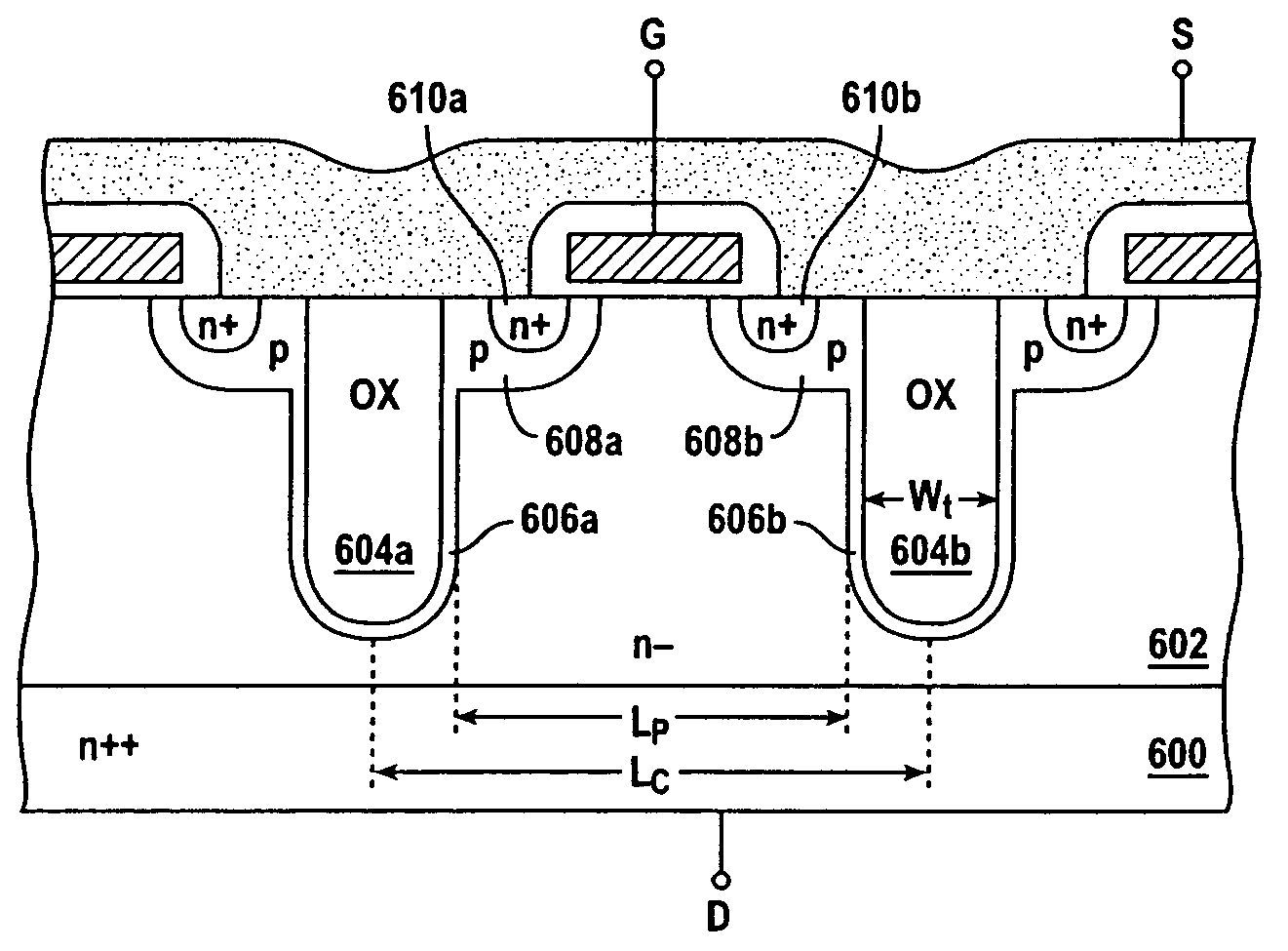
[0037]FIG. 2 shows a cross-sectional view of a power MOSFET cell array in accordance with an embodiment of the present invention. As shown, both gate terminal 205 and source terminal 207 are located along the top-side of the device, and drain terminal 203 is located along the bottom-side. Drain terminal 203 is coupled to the lightly-doped epitaxial region 202 through a highly doped region 200 serving as the drain contact. Oxide-filled trench regions 204a, 204b extend from the top-side to a predetermined depth in the epitaxial region 202. Discontinuous floating p-type regions 206a, 206b are spaced along an outer sidew...


PUM


Abstract

In accordance with an embodiment of the present invention, a MOSFET includes at least two insulation-filled trench regions laterally spaced in a first semiconductor region to form a drift region therebetween, and at least one resistive element located along an outer periphery of each of the two insulation-filled trench regions. A ratio of a width of each of the insulation-filled trench regions to a width of the drift region is adjusted so that an output capacitance of the MOSFET is minimized.

Description

CROSS-REFERENCE TO RELATED APPLICATIONS[0001]This application is a division of and claims priority to U.S. application Ser. No. 10 / 200,056, filed Jul. 18, 2002 now U.S. Pat. No. 6,803,626, which disclosure is incorporated herein by reference for all purposes.BACKGROUND OF THE INVENTION[0002]Power field effect transistors, e.g., MOSFETs (metal oxide semiconductor field effect transistors), are well-known in the semiconductor industry. One type of power MOSFET is a DMOS (double-diffused metal oxide semiconductor) transistor. A cross-sectional view of a portion of a cell array of one known variety of DMOS transistors is shown in FIG. 1. As shown, an n-type epitaxial layer 102 overlies n-type substrate region 100 to which the drain contact is made. Polysilicon-filled trenches extend into the epitaxial layer 102 from the top surface. The polysilicon 106a, 106b in the trenches are insulated from the epitaxial layer by oxide layers 104a, 104b. Source regions 108a, 108b in p-type body regio...

Claims


Application Information

Patent Timeline
Patent Type & Authority Patents(United States)
IPC IPC(8): H01L29/00H01L29/76H01L29/94H01L31/062H01L31/113H01L29/06H01L29/40H01L29/78
CPCH01L29/0634H01L29/7813H01L29/407H01L29/7802H01L29/0619H01L29/0649H01L29/405H01L29/0653H01L29/7811
Inventor SAPP, STEVENWILSON, PETER H.
Owner SEMICON COMPONENTS IND LLC
Why Eureka
Try Eureka