

Functional film for transfer having functional layer, object furnished with functional layer and process for producing the same
a functional layer and functional film technology, applied in the direction of conductive layers on insulating supports, thermography, instruments, etc., can solve the problems of large apparatus, slow layer forming speed, and inability to form a large area of layers, so as to achieve uniform thickness and lower electric resistance
- Summary
- Abstract
- Description
- Claims
- Application Information
AI Technical Summary
Benefits of technology
Problems solved by technology
Method used
Image

Examples
example 1
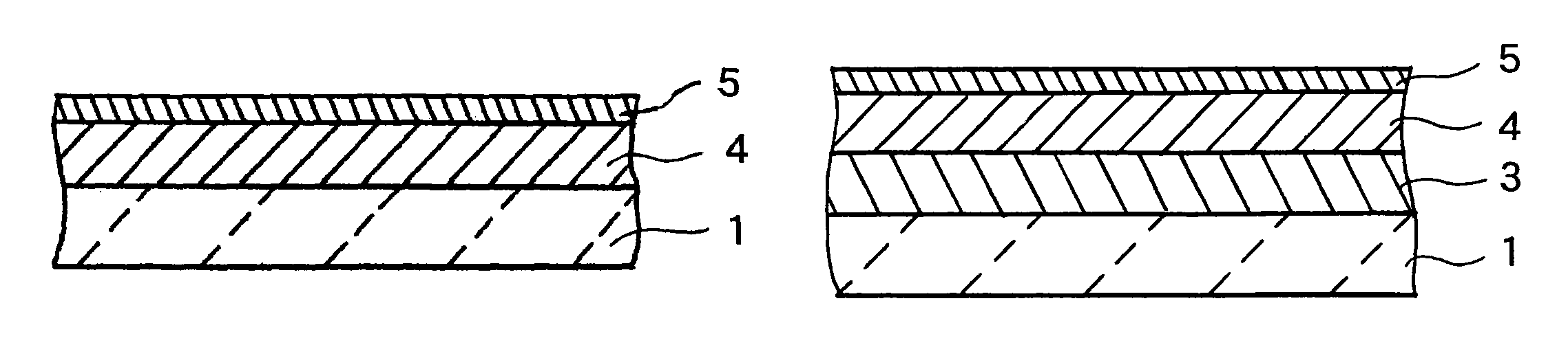
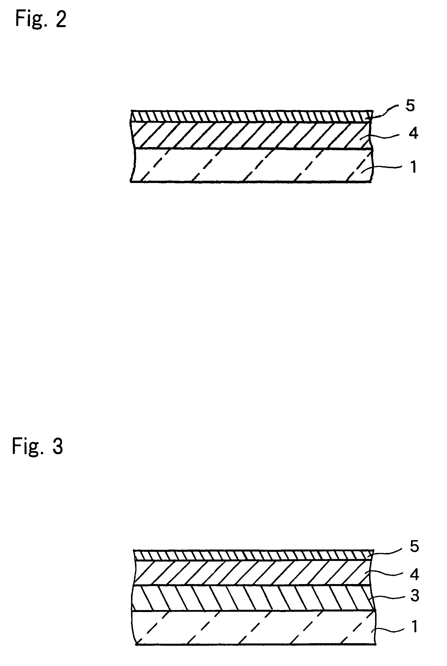
[0148]A conductive film for transfer of the second type having, on a support (1), a resin layer (3), a conductive layer (4) and an adhesive layer (5) in this order was produced, as illustrated in FIG. 3.
(Formation of Hard Resin Layer)
[0149]A PET film (1) having a thickness of 75 μm (HSL, produced by Teijin Dupont Films Ltd.) was subjected to corona treatment so that the contact angle thereof with pure water was made into 39°. 100 parts by weight of an A solution of FRESCERA. N (produced by Matsushita Electric Industrial Co., Ltd.) were mixed with 300 parts by weight of a B solution thereof to prepare a coating solution for a resin layer. The coating solution was applied onto the corona-treated surface of the PET film (1), dried and cured at 90° C. for 24 hours to form a silicone resin layer (3) having a thickness of 1 μm.
(Formation of Conductive Layer)
[0150]To 100 parts by weight of ITO fine particles, SUFP-HX (produced by Sumitomo Metal Mining Co., Ltd.) having a primary particle d...
example 2
[0159]A conductive film for transfer was obtained in the same way as in Example 1 except that the composition of the coating solution for adhesive layer was made as follows:[0160]acrylic type resin 103B: 90 parts by weight,[0161]ultraviolet curable resin SD-318: 50 parts by weight,[0162]the above-mentioned silicone resin solution: 12.5 parts by weight, and methyl ethyl ketone: 181 parts by weight.
When the adhesive layer of the resultant conductive film for transfer was fingered, tackiness was felt. The resultant conductive film for transfer was used to transfer the conductive layer onto a glass plate and the calcining was performed in the same way as in Example 1. The adhesive layer (5) was very strong after the curing also. The electric resistance of the conductive layer (4) was 100 Ω / ▭.
example 3
[0163]A conductive film for transfer was obtained in the same way as in Example 1 except that the composition of the coating solution for adhesive layer was made as follows:[0164]acrylic type resin 103B: 80 parts by weight,[0165]ultraviolet curable resin SD-3 18: 50 parts by weight,[0166]the above-mentioned silicone resin solution: 25 parts by weight, and methyl ethyl ketone: 178 parts by weight.
When the adhesive layer of the resultant conductive film for transfer was fingered, tackiness was felt. The resultant conductive film for transfer was used to transfer the conductive layer onto a glass plate and the calcining was performed in the same way as in Example 1. The adhesive layer (5) was very strong after the curing also. The electric resistance of the conductive layer (4) was 100 Ω / ▭.
PUM
| Property | Measurement | Unit |
|---|---|---|
| temperature | aaaaa | aaaaa |
| temperature | aaaaa | aaaaa |
| temperature | aaaaa | aaaaa |
Abstract
Description
Claims
Application Information