Method for fabricating silicon nitride spacer structures

a technology of silicon nitride and spacers, applied in the field of depositing methods of siliconbased materials, can solve the problems of extended duration, limited interfacing requirements, and difficult task of fabricating spacer structures

Active Publication Date: 2007-11-13
APPLIED MATERIALS INC
View PDF11 Cites 398 Cited by
  • Summary
  • Abstract
  • Description
  • Claims
  • Application Information

AI Technical Summary

Problems solved by technology

Fabrication of spacer structures represents a challenging task and often the interfacing requirements are only partially met, or are met at the expense of low yield.
In addition, present manufacturing techniques utilize different processing tools, resulting in extended duration and high cost of fabricating the spacer structures.

Method used


Image

  • Method for fabricating silicon nitride spacer structures
  • Method for fabricating silicon nitride spacer structures
  • Method for fabricating silicon nitride spacer structures

Examples


Embodiment Construction

[0014]The present invention is generally a method for fabricating spacer structures in integrated semiconductor circuits and devices.

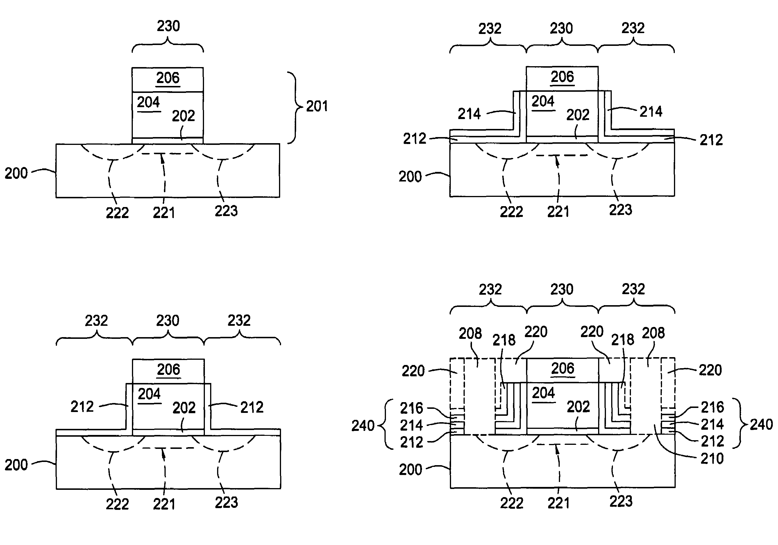
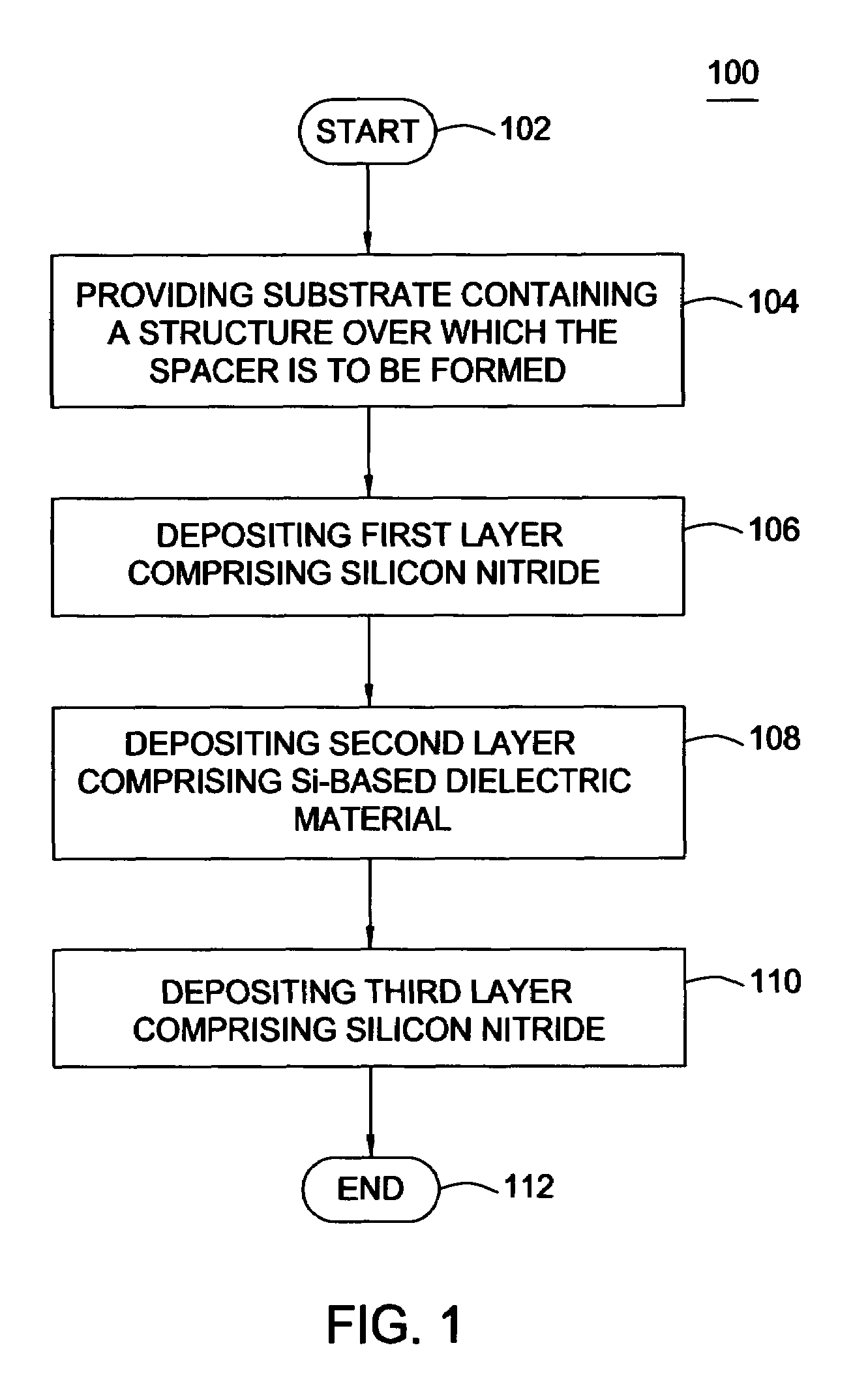
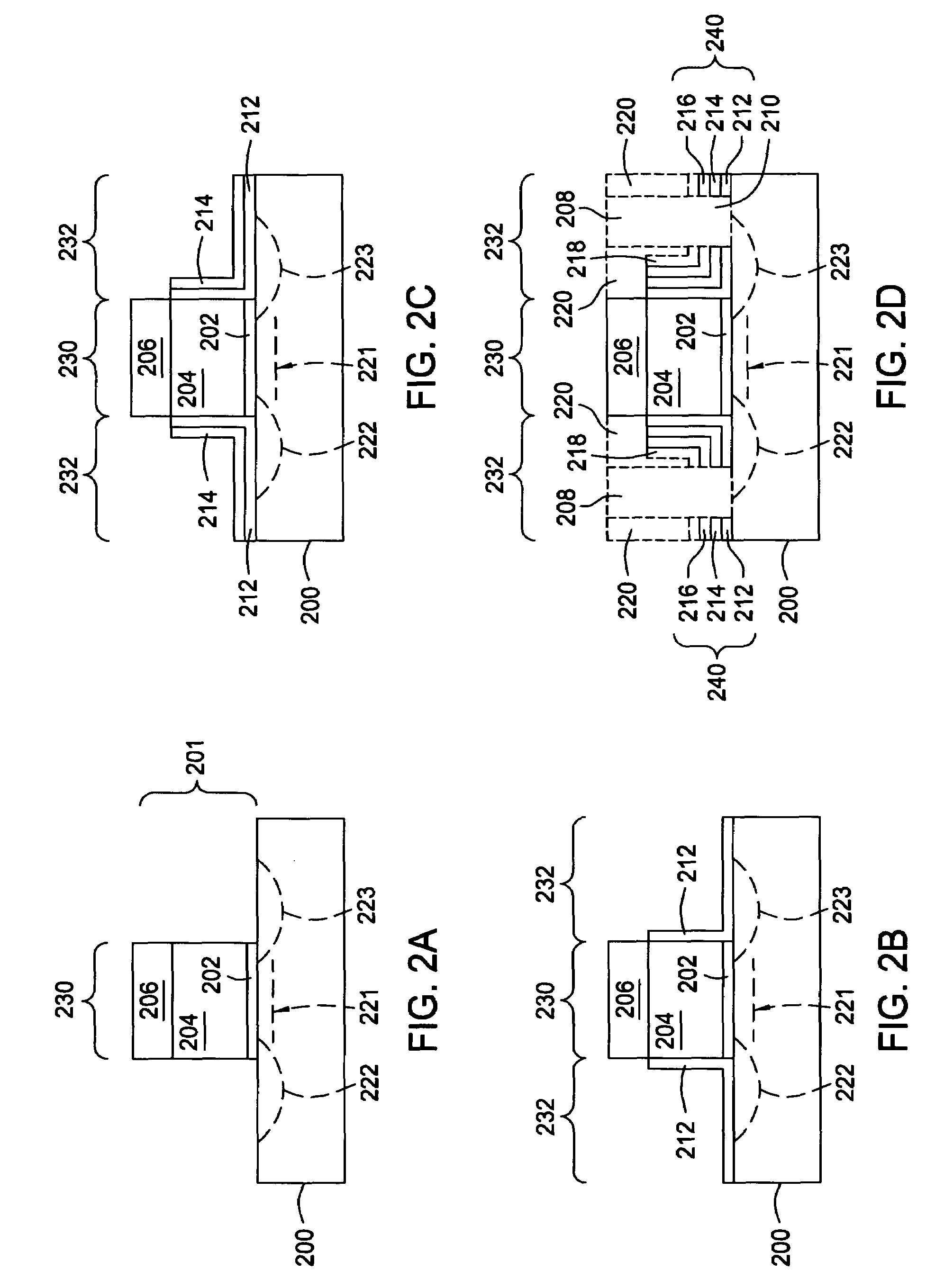
[0015]FIG. 1 depicts a flow diagram illustrating a method 100 for fabricating a spacer structure over a desired feature of a substrate in accordance with one embodiment of the present invention. The method 100 includes processing steps performed upon a substrate during fabrication of the spacer structure. Sub-steps and auxiliary procedures (e.g., process control sub-steps, lithographic routines, and the like) are well known in the art and, as such, are omitted herein. Spacer structures formed as described in the method 100 are suitable for use in connection with the fabrication of, for example, field effect transistors (FET), dynamic random access memory (DRAM), flash memory, and the like.

[0016]The steps of the method 100 can be performed using a low pressure chemical vapor deposition (LPCVD) reactor, among other suitable processing reactors known to t...


PUM

PropertyMeasurementUnit
thickaaaaaaaaaa
thickaaaaaaaaaa
thicknessaaaaaaaaaa

Abstract

Embodiments of methods for fabricating a spacer structure on a semiconductor substrate are provided herein. In one embodiment, a method for fabricating a spacer structure on a semiconductor substrate includes providing a substrate containing a base structure over which the spacer structure is to be formed. The spacer structure may be formed over the base structure by depositing a first layer comprising silicon nitride on the base structure, depositing a second layer comprising a silicon-based dielectric material on the first layer, and depositing a third layer comprising silicon nitride on the second layer. The first, second, and third layers are deposited in a single processing reactor.

Description

BACKGROUND OF THE INVENTION[0001]1. Field of the Invention[0002]Embodiments of the invention generally relate to methods for depositing silicon-based materials. More specifically, the present invention relates to chemical vapor deposition techniques for fabricating multi-layer silicon nitride spacer structures.[0003]2. Description of the Related Art[0004]A spacer structure is an integral part of many devices formed on an integrated circuit (IC). In one example, spacer structures may be utilized in a field effect transistor (e.g., a complementary metal-oxide-semiconductor (CMOS) field effect transistor, and the like) to insulate and protect gate structures of the transistor from materials disposed adjacent to the gate structure. The spacer structure is disposed between various dielectric and conductive layers of the transistor and has complex interfacing requirements, for example, diffusion and barrier characteristics, intrinsic stress, bond strength, material compatibility, and the ...

Claims


Application Information

Patent Timeline
Patent Type & Authority Patents(United States)
IPC IPC(8): H01L21/30
CPCH01L21/0214H01L21/02164H01L21/0217H01L21/022H01L29/6656H01L21/3144H01L21/3145H01L21/31612H01L21/3185H01L21/02271
Inventor IYER, R. SURYANARAYANANTANDON, SANJEEV
Owner APPLIED MATERIALS INC
Why Eureka
Try Eureka