Method of fabricating dielectric mixed layers and capacitive element and use thereof

a technology of capacitive elements and dielectric mixed layers, which is applied in the direction of capacitors, semiconductor devices, electrical apparatuses, etc., can solve the problems of placing limits on conventional methods, and achieve the effect of improving thermal stability and increasing capacitan

Inactive Publication Date: 2007-12-04
POLARIS INNOVATIONS LTD
View PDF9 Cites 12 Cited by
  • Summary
  • Abstract
  • Description
  • Claims
  • Application Information

AI Technical Summary

Benefits of technology

[0005]Therefore, it is an object of the present invention to provide a capacitive element with an increased capacitance in conjunction with an improved thermal stability.
[0010]Consequently, the method according to the invention has the advantage that it is possible to produce an improved dielectric, i.e. a dielectric layer with an increased dielectric constant k in conjunction with an improved thermal stability.
[0036]In accordance with yet another preferred development of the present invention, the dielectric mixed layer has a dielectric constant (k) that is altered with respect to the dielectric layer. The dielectric constant (k) of the dielectric mixed layer is preferably increased with respect to that of the dielectric layer, or the mixed layer has an increased thermal stability.
[0038]Furthermore, it is advantageous to form the dielectric mixed layer multiply (n times) on one another in order to obtain a dielectric layer stack.

Problems solved by technology

In an inexpedient manner, limits are placed on the conventional methods in the case of increasing the dielectric constant and also in the case of the thermal stability of the dielectric layer.

Method used


Image

  • Method of fabricating dielectric mixed layers and capacitive element and use thereof
  • Method of fabricating dielectric mixed layers and capacitive element and use thereof
  • Method of fabricating dielectric mixed layers and capacitive element and use thereof

Examples


Embodiment Construction

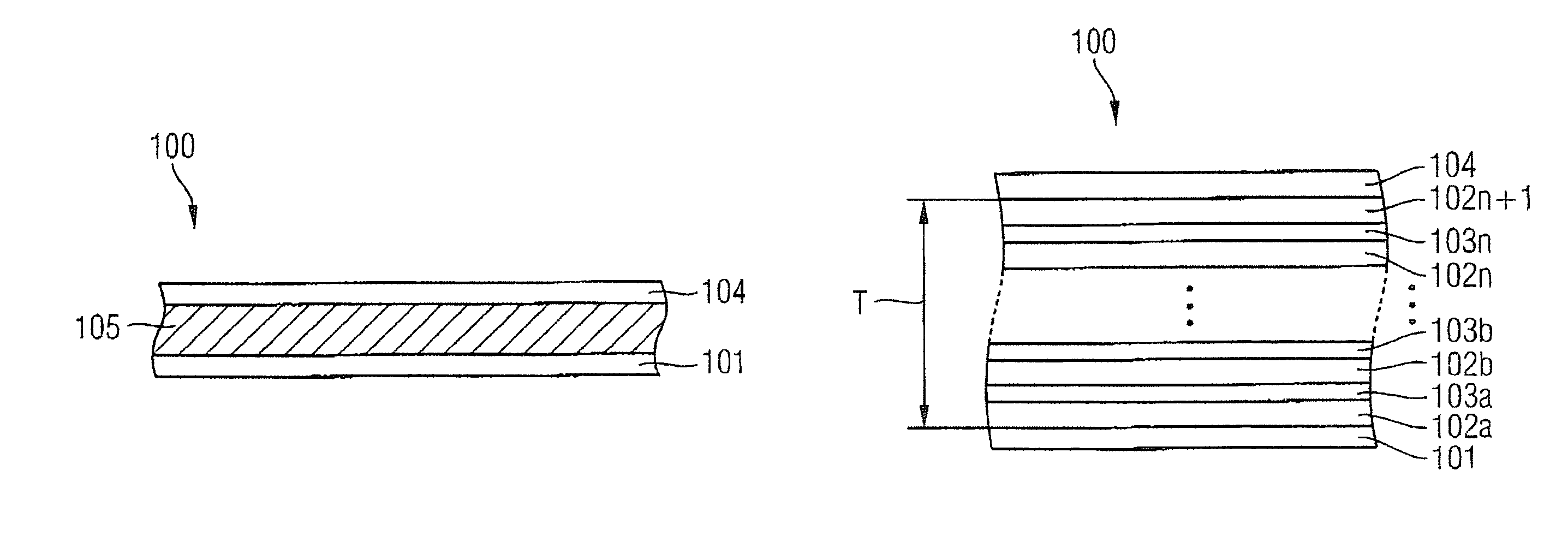
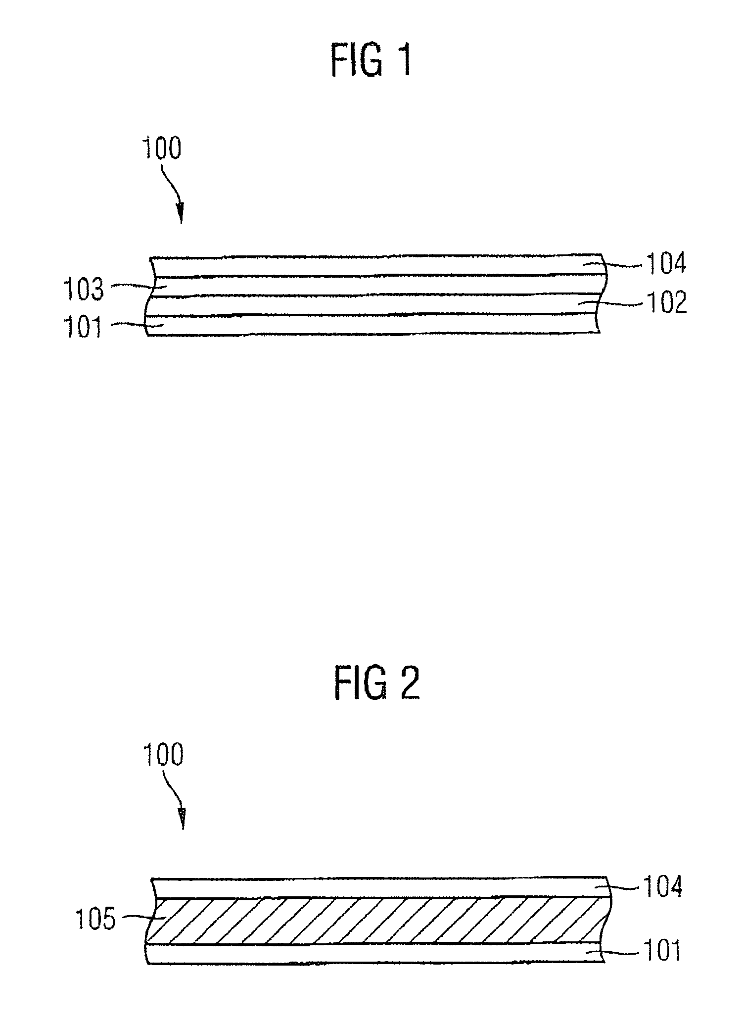
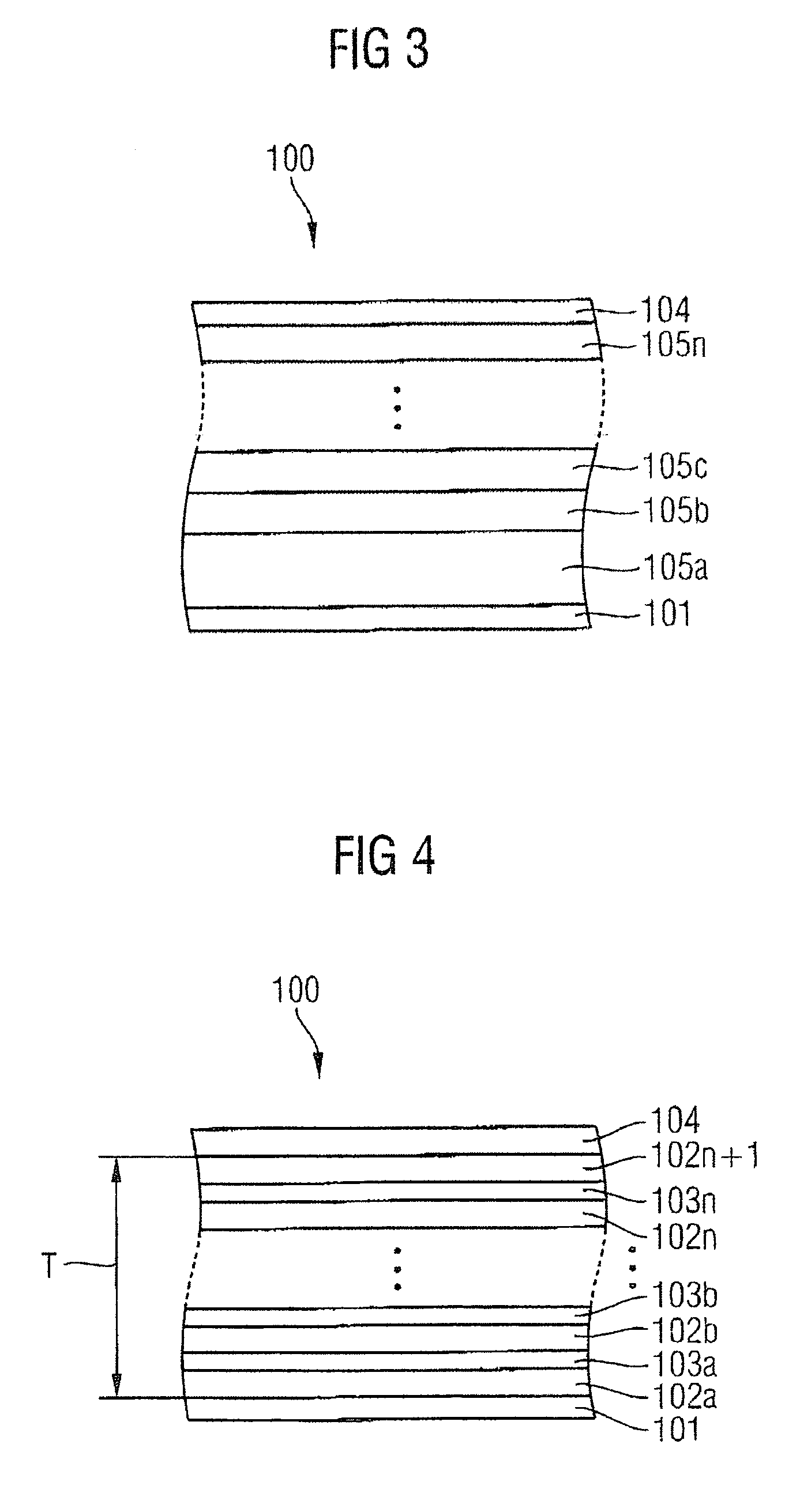
[0044]In the figures, identical reference symbols designate identical or functionally identical components or steps.

[0045]The capacitive element 100 shown in FIG. 1 has a substrate 101 provided as a first electrode layer of the capacitive element 100, a dielectric layer 102 being applied on said substrate. Before the dielectric layer 102 is applied to the substrate 101, the latter is conditioned for example by means of a heat treatment in various ambient gas atmospheres or by means of conventional wet-chemical methods. Conditioning means, in particular, that, if the substrate 101 comprises silicon, silicon oxide (SiO2) or SiN or SiON is excited on the surface in order to facilitate the further layer construction process.

[0046]FIG. 1 schematically shows the layer sequence for the capacitive element 100, while FIG. 2 illustrates an arrangement according to the invention for the capacitive element 100, in such a way that a mixed layer 105 is formed by a heat treatment step. In order to...


PUM

PropertyMeasurementUnit
relative permittivityaaaaaaaaaa
dielectric constantaaaaaaaaaa
capacitanceaaaaaaaaaa

Abstract

The present invention provides a method for fabricating a capacitive element (100), a substrate (101) being provided as a first electrode layer of the capacitive element (100), the substrate (101) provided as an electrode layer is conditioned, a dielectric layer (102) is deposited on the conditioned substrate (101) and a second electrode layer (104) is applied on the layer stack produced, the layer stack being modified by a heat treatment in such a way that the dielectric layer (102) deposited on the conditioned substrate (101) forms a dielectric mixed layer (105) with a reaction layer (103) deposited on the dielectric layer (102), which dielectric mixed layer has an increased dielectric constant (k) or an increased thermal stability.

Description

TECHNICAL FIELD[0001]The present invention generally relates to the field of miniaturized capacitive elements contained in electronic circuit units (electronic chips). Capacitive elements of this type require dielectrics (dielectric layers) having a highest possible relative permittivity or dielectric constant k.BACKGROUND ART[0002]In particular, the present invention relates to a method for fabricating a capacitive element in which a substrate is provided, which substrate serves as a first electrode layer of the capacitive element, in which the substrate provided as a first electrode layer is conditioned, in which a dielectric layer is deposited on the conditioned substrate, and in which a second electrode layer is subsequently applied.[0003]Conventional dielectric layers for capacitive elements disadvantageously have a low dielectric constant k. Reoxidized nitrides (NO) are usually used in the fabrication of capacitive elements. In order to increase the dielectric constant k of th...

Claims


Application Information

Patent Timeline
Patent Type & Authority Patents(United States)
IPC IPC(8): H01L21/20H01L21/02H01L21/316H01L21/822H01L21/8242H01L27/08H01L29/76
CPCH01L28/56H01L21/31604H01L21/31608H01L21/31641H01L21/31645H01L21/31637H01L21/022
Inventor GUTSCHE, MARTINSEIDL, HARALD
Owner POLARIS INNOVATIONS LTD
Why Eureka
Try Eureka