Package for electronic device, base substrate, electronic device and fabrication method thereof

Inactive Publication Date: 2007-12-04
TAIYO YUDEN KK
View PDF8 Cites 10 Cited by
  • Summary
  • Abstract
  • Description
  • Claims
  • Application Information

AI Technical Summary

Benefits of technology

[0009]It is a general object of the present invention to provide an electronic device that can be simply fabricated and to provide a fabrication method thereof.
[0010]A further object of the present invention is to provide a package for such an electronic device and a base substrate.

Problems solved by technology

However, the above conventional method has the following disadvantage.

Method used


Image

  • Package for electronic device, base substrate, electronic device and fabrication method thereof
  • Package for electronic device, base substrate, electronic device and fabrication method thereof
  • Package for electronic device, base substrate, electronic device and fabrication method thereof

Examples


first embodiment

[0033]A first embodiment of the present invention is directed to a SAW device.

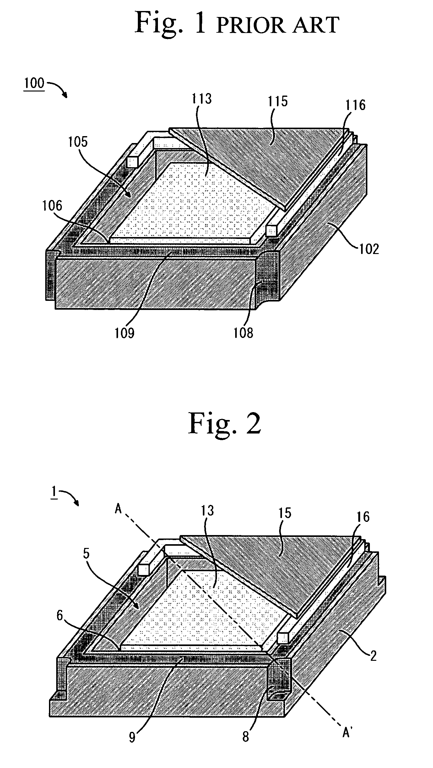
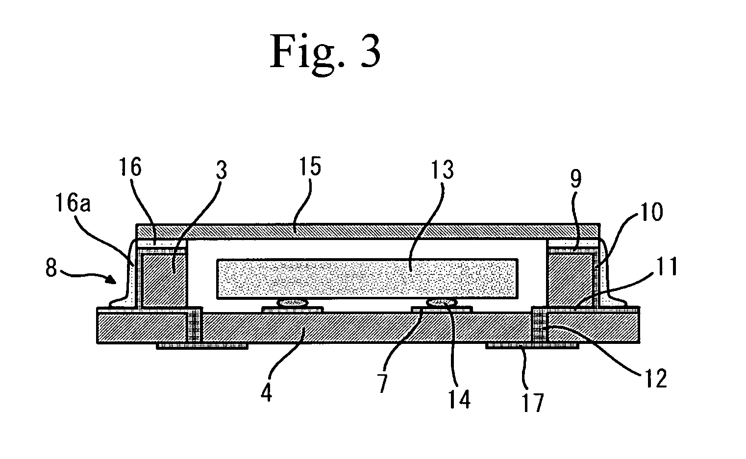
[0034]FIG. 2 is a perspective view of a SAW device 1 according to the present embodiment. The SAW device 1 has a SAW chip 13 having a piezoelectric substrate on which an interdigital transducer (IDT) having comb-like electrodes is formed. The SAW chip 13 is housed in a cavity 5 of a package 2. A wiring pattern (die attach pattern 7, see FIG. 3) is formed on the bottom surface of the cavity 5 (die attach surface 6). The die attach pattern 7 has the major component of aluminum, copper, gold, molybdenum, tungsten, tantalum, chromium, titanium, platinum, ruthenium or rhodium. The SAW chip 13 is flip-chip mounted so that the IDTs face the bottom of the cavity (face-down mounting). The die attach pattern 7 and the SAW chip 13 are bonded together with bumps 14 (see FIG. 3), which is made of a conductive material of, for example, gold, aluminum or cupper as the major component, so that these parts are electrically...

second embodiment

[0047]A description will now be given of a second embodiment of the present invention with reference to the accompanying drawings.

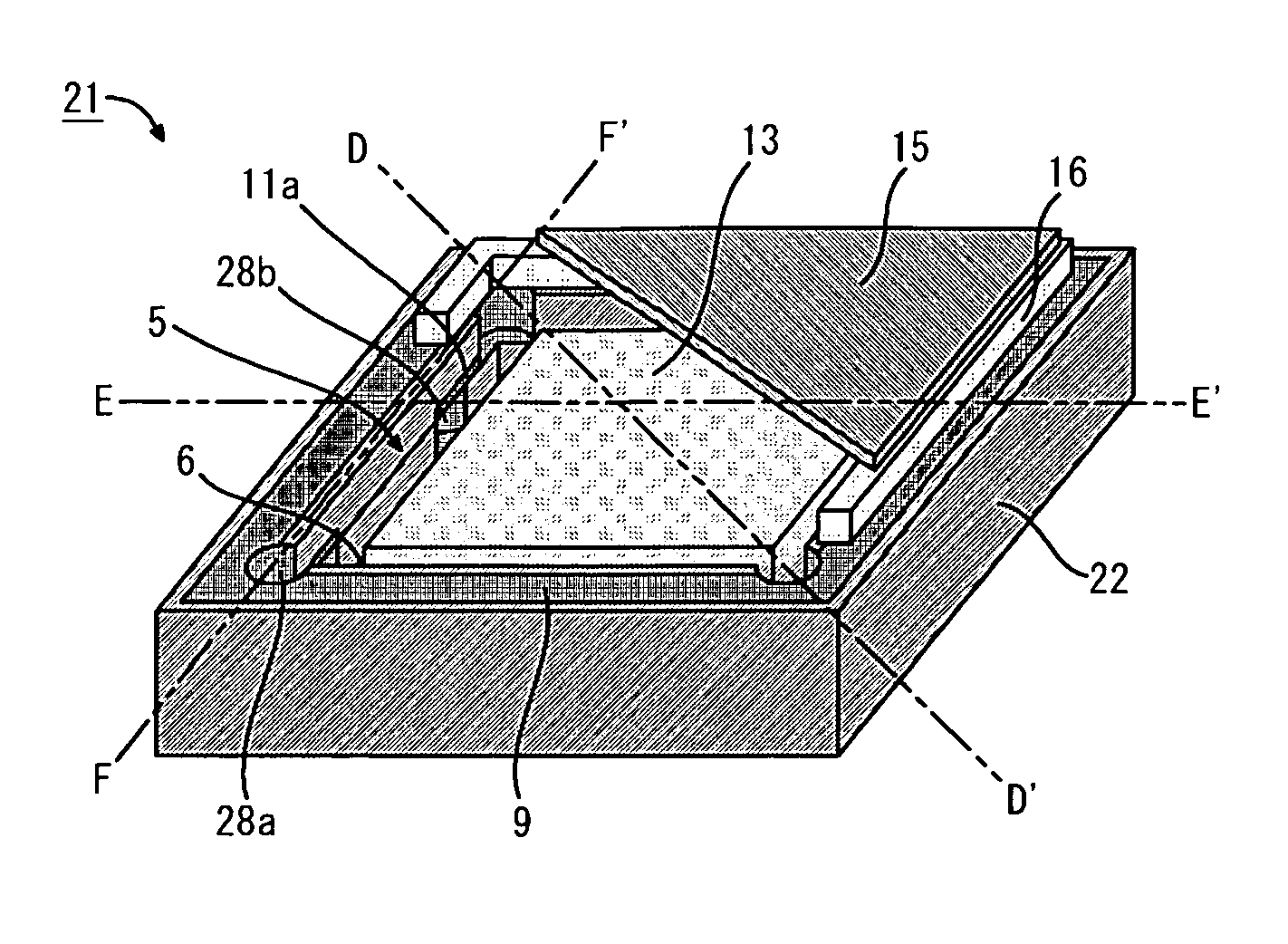
[0048]In the above-mentioned first embodiment, the castellations 8 are formed on the outer surfaces of the sidewalls of the package 2. In contrast, the second embodiment employs an arrangement shown in FIG. 6 in which castellations 28a and 28b are formed on the inner surfaces of the sidewalls of a package 22, namely, the inner walls of the cavity 5.

[0049]FIG. 6 shows a SAW 21 of the present embodiment. As shown in FIG. 6, castellations 28a and 28b that have a two-stage structure are formed on the inner walls of the cavity 5, and have plating layers 10a and 10b formed on the surfaces thereof, respectively. The plating layers 10a and 10b (see FIGS. 7 and 8) are electrically connected each other via a wiring pattern 11a. This configuration will be explained below in more detail with reference to FIGS. 7 through 9.

[0050]FIG. 7 is a cross-sectional view taken ...

third embodiment

[0061]Next, a third embodiment of the present invention will now be explained with reference to the accompanying drawings.

[0062]In the first and second embodiments, the castellations for retaining the flowed-out washer and preventing short-circuiting on the package backside or the cavity bottom are provided on the sidewalls of the package (more particularly, the inner and outer surfaces of the sidewalls). In contrast, the third embodiment employs holes in the sidewalls, which holes do not penetrate the sidewalls.

[0063]FIG. 11 is a perspective view of a SAW device 31 according to the third embodiment. As shown in FIG. 11, holes 38 are formed in sidewalls of a package 32 that define the cavity 5, more specifically, in the upper layer substrate 3 so as to penetrate the substrate 3. The inner surfaces of the holes 38 are plated. This configuration is explained in more detail with reference to FIG. 12.

[0064]FIG. 12 is a cross-sectional view taken along a line J–J′ shown in FIG. 11. As sh...


PUM


Abstract

A package for an electronic device includes a cavity that houses an electronic element, and grooves or holes formed on or in sidewalls that define the cavity. The grooves or holes extend from an open side of the cavity so as not to reach a bottom side of the package.

Description

BACKGROUND OF THE INVENTION[0001]1. Field of the Invention[0002]The invention generally relates to a package for an electronic device, a base substrate, an electronic device, and a fabrication method thereof.[0003]2. Description of the Related Art[0004]Recently, there has been a demand to downsize electronic elements mounted to electronic devices and improve the performance thereof with downsizing and high performance of the electronic devices. For instance, there have been similar demands on surface acoustic wave (SAW) devices that are electronic parts used as filters, delay lines, oscillators in electronic devices capable of transmitting and receiving radio waves.[0005]Generally, SAW devices have a SAW filter chip that is flip-chip mounted within a cavity having a bottom surface on which interconnection lines are formed. An interdigital transducer (IDT) having comb-like electrodes is formed on a piezoelectric substrate of the SAW filter chip. This type of SAW devices is disclosed ...

Claims


Application Information

Patent Timeline
IPC IPC(8): H01L41/08H01L23/04H03H9/08H03H9/25
CPCH03H9/1071H03H9/08H01L2224/16225H01L2224/97H01L2924/16195H01L2924/16315H01H9/16H01H23/025B82Y25/00H01H2219/036F21Y2101/00H01H2219/014
Inventor MASUKO, SHINGOKAWACHI, OSAMUKOORIIKE, TAKUMI
Owner TAIYO YUDEN KK
Why Eureka
Try Eureka