High radiance LED chip and a method for producing same

a technology of led chips and radiance, applied in the direction of basic electric elements, electrical equipment, semiconductor devices, etc., can solve the problems of high reflection loss, failure to find widespread application, and opaque casting compounds, so as to prevent losses, and increase the luminous efficiency

Inactive Publication Date: 2007-12-11
OSRAM GMBH
View PDF31 Cites 26 Cited by
  • Summary
  • Abstract
  • Description
  • Claims
  • Application Information

AI Technical Summary

Benefits of technology

[0028]A further advantageous embodiment of the invention provides that the light-emission-limiting system takes the form of an insulating layer that is realized on or at the active layer and between the active layer and a power supply, and that minimizes the supply of power or flow of current to and through the active layer in the regions outside the light-emitting region. Here again, the active layer can extend as a continuous layer within a wafer that nevertheless contains many individual light-emitting semiconductor components.
[0029]The insulating layer is advantageously a nonconductive oxide layer deposited on the side of the window layer opposite the light exit surface. The masking of the power supply can thus be achieved in a particularly simple and inexpensive manner. The oxide layer is advantageously produced by oxidizing the material that is already present.
[0035]The power supplies and / or the insulating layer are advantageously reflective of the emitted light. This further increases the luminous efficiency by preventing losses.
[0036]A reflecting device for the emitted light is advantageously realized in or on the window layer or active layer, on the side of the active layer facing away from the light exit surface. Again, this brings about a further increase in luminous efficiency by preventing losses. The reflecting device is accordingly a Bragg lattice.
[0037]In a further embodiment of the invention, the window layer and / or the optical device are provided, at least in part, with a covering that is transparent to the emitted light. The light-emitting semiconductor component is thereby protected against environmental influences. This permits external shaping to suit numerous applications.

Problems solved by technology

Also known is the use of high-refractive, transparent casting compounds; however, these have failed to find widespread application because of cost considerations, among other factors.
Moreover, the best casting compounds available heretofore have had a refractive index n of no more than 1.6, resulting in too large a jump at the decoupling surface of the light-emitting semiconductor component, and thus high reflection losses.
In addition, the highly transparent casting compounds have undesirable chemical and mechanical properties, which also limits their large-scale industrial application.

Method used


Image

  • High radiance LED chip and a method for producing same
  • High radiance LED chip and a method for producing same
  • High radiance LED chip and a method for producing same

Examples


Embodiment Construction

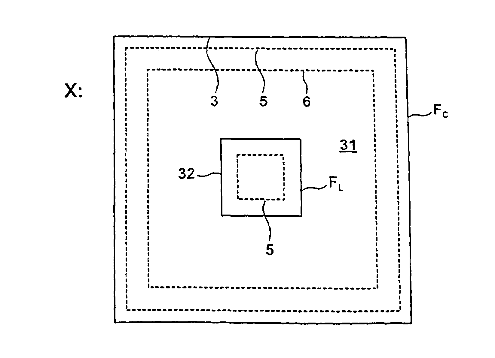
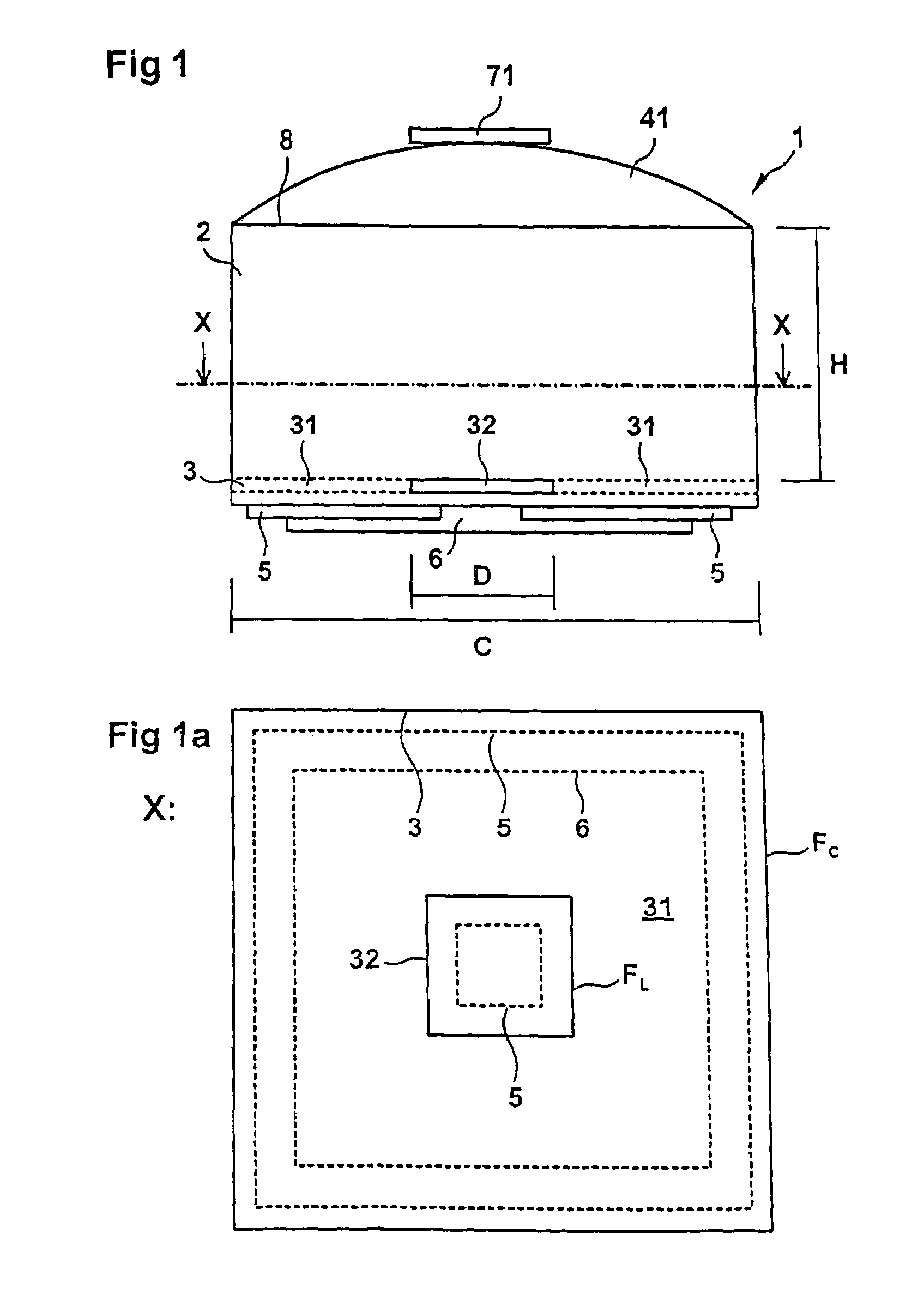
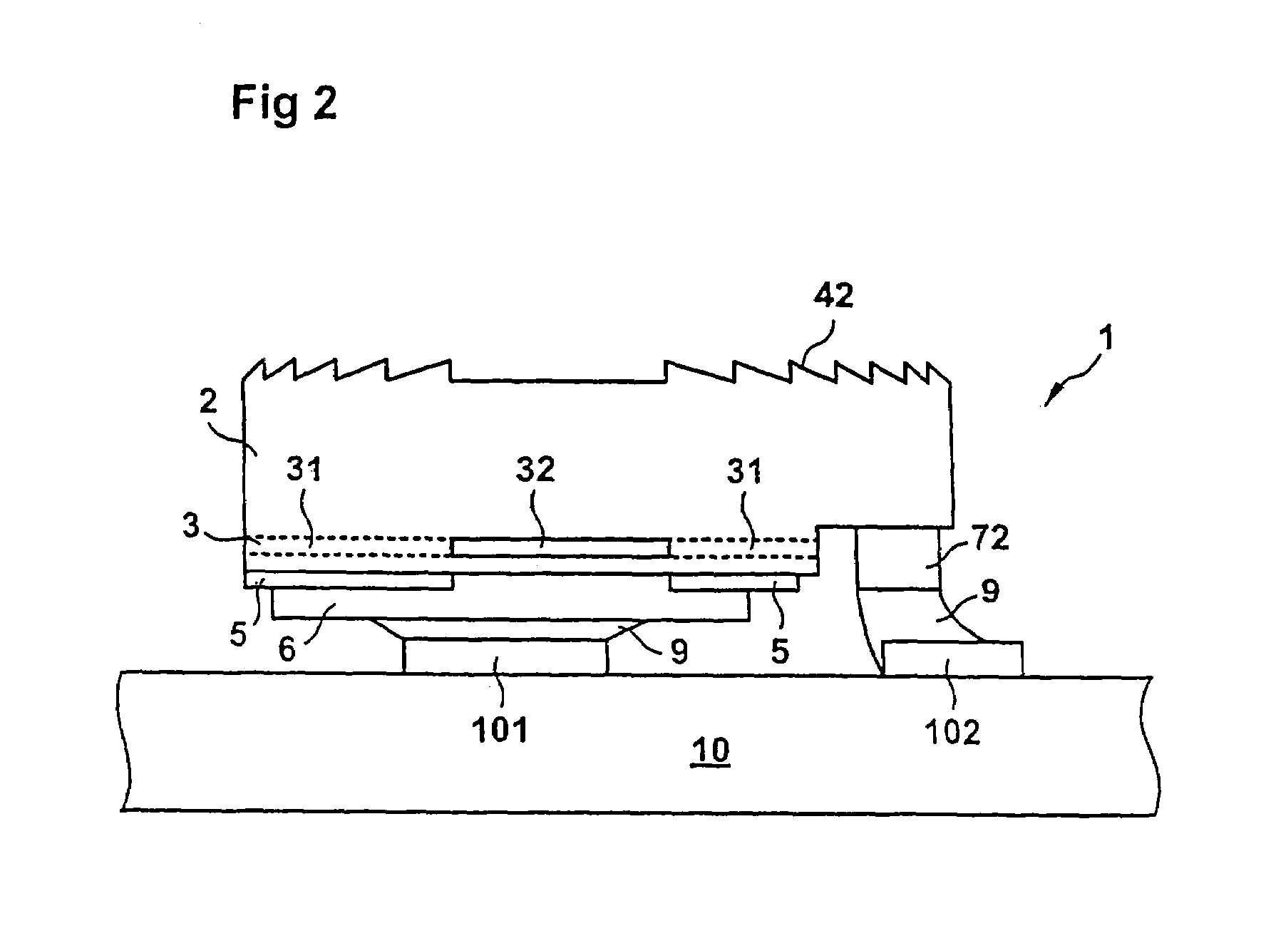
[0051]The light-emitting region 32 of active layer 3 is limited and defined with respect to size and shape by masking of the insulating layer 5. The shape of the electrical insulation makes it possible for power supply 6, which is realized areally on the bottom side of light-emitting semiconductor component 1 disposed opposite light exit surface 8, to contact the chip or the active layer at those locations above which the light-emitting region 32 is situated. In the example, the material used for the insulating layer is an oxide layer [sic]. The power supply 6 can in this case be realized by means of metal deposited areally over the insulating layer 5. Thus, no current flows through the regions 31 of active layer 3 not intended for emission, and consequently no emission of light takes place in these regions. The second current entry is effected by means of first power supply 71, which is realized on the electrically conductive lens 41 in the form of an electrical contact (“pad”) and...


PUM


Abstract

The invention concerns a light-emitting diode chip comprising a radiation-emitting active region and a window layer. To increase the luminous efficiency, the cross-sectional area of the radiation-emitting active region is smaller than the cross-sectional area of the window layer available for the decoupling of light.The invention is further directed to a method for fabricating a lens structure on the surface of a light-emitting component.

Description

CROSS REFERENCE TO RELATED APPLICATIONS[0001]This application is a divisional of U.S. application Ser. No. 10 / 258,154, filed Oct. 18, 2002, which is a National Phase application for PCT International Application No. PCT / DE01 / 01513, field Apr. 19, 2001, which claims priority to German Application No. DE 100 19 665.9, filed Apr. 19, 2000. The contents of the prior applications are incorporated herein by reference in their entirety.FIELD OF THE INVENTION[0002]The invention relates to a light-emitting diode chip and a fabrication method thereof.BACKGROUND OF THE INVENTION[0003]Semiconductor materials for light-emitting diode (LED) chips have a refractive index that in some cases is well above 3. The refractive index of the medium adjacent the chip in conventional LED components—usually air or plastic—is much lower. The associated sharp jump in refractive index at the interface between the LED chip and the adjacent medium makes for a comparatively small critical angle for total reflectio...

Claims


Application Information

Patent Timeline
Patent Type & Authority Patents(United States)
IPC IPC(8): H01L21/00H01L33/02H01L33/08H01L33/14H01L33/20H01L33/44
CPCH01L33/02H01L33/08H01L33/20H01L2224/16225H01L33/44H01L33/145
Inventor BOGNER, GEORGKUGLER, SIEGMARNIRSCHL, ERNSTOBERSCHMID, RAIMUNDSCHLERETH, KARL-HEINZSCHOENFELD, OLAFSTATH, NORBERTNEUMANN, GERALD
Owner OSRAM GMBH
Why Eureka
Try Eureka