High frequency switch device

a high-frequency switch and switch technology, applied in the direction of electronic switching, pulse technique, electrical apparatus, etc., can solve the problems of insufficient cost reduction, insufficient cost reduction, increased chip area, etc., and achieve the effect of simple circuit configuration and improved isolation characteristi

Active Publication Date: 2007-12-11
MITSUBISHI ELECTRIC CORP +1
View PDF12 Cites 64 Cited by
  • Summary
  • Abstract
  • Description
  • Claims
  • Application Information

AI Technical Summary

Benefits of technology

[0018]The present invention has been made to solve the foregoing problems. A first object of the present invention is to provide a small-sized high frequency switch device which improves an isolation characteristic in a simple circuit configuration.
[0020]Accordingly, in the high frequency switch device according to the present invention, the number of control pins is reduced to enable its size reduction. An isolation characteristic is enhanced owing to such a simple configuration that second ports of SPDTs are connected to their corresponding terminating resistors, and a reflection variation in input signal, i.e., variations in the intensity and phase of the input signal can be lessened owing to the effects of the terminating resistors upon input changeover to first and second SPDT switches, thereby making it possible to suppress adverse effects exerted on other circuits.

Problems solved by technology

Thus, a chip area increased and a reduction in cost could not be achieved sufficiently.
Since a logic circuit of a decoder IC unit is fine and complex as compared with the switch unit, process yields are reduced and hence a reduction in cost could not be achieved sufficiently due to the reduction in the yield.
Therefore, the N×M switch resulted in upsizing of a chip and a package and an increase in cost.
Further, when a plurality of switch elements are connected in tournament form to reduce the number of the control pins, the setting of impedance of each connecting wiring becomes complex to realize high isolation of the high frequency switch, so an increase in complexity of a circuit configuration cannot be avoided.
Such a high frequency circuit that a circuit configuration on a chip is greatly affected by its electric characteristic, unavoidably resulted in a reduction in the degree of freedom of circuit design.
As described above, the conventional high frequency switch is accompanied by the problems that when the decoder circuit is added thereto, its size reduction and low cost cannot be achieved, whereas when no decoder circuit is added, the number of the control pins increases, thus resulting in upsizing of the chip and package and the increase in cost, and when an attempt is made to reduce the number of the control pins and achieve high isolation, the setting of impedance in the circuit becomes complex and the degree of freedom of design is degraded, for example.

Method used


Image

  • High frequency switch device
  • High frequency switch device
  • High frequency switch device

Examples


first embodiment

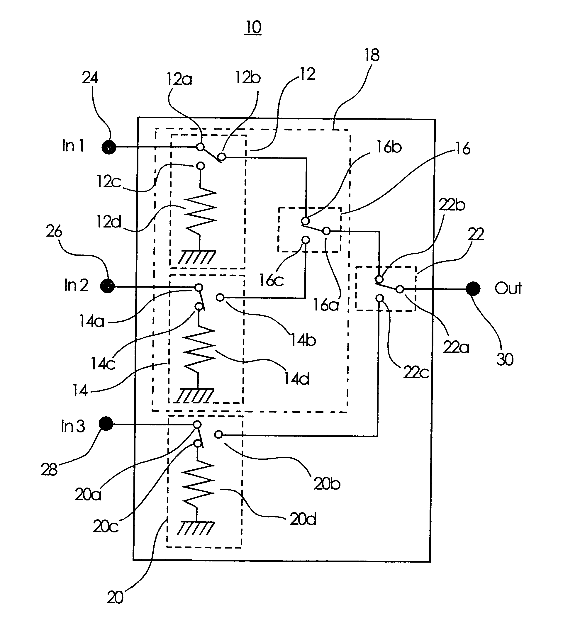
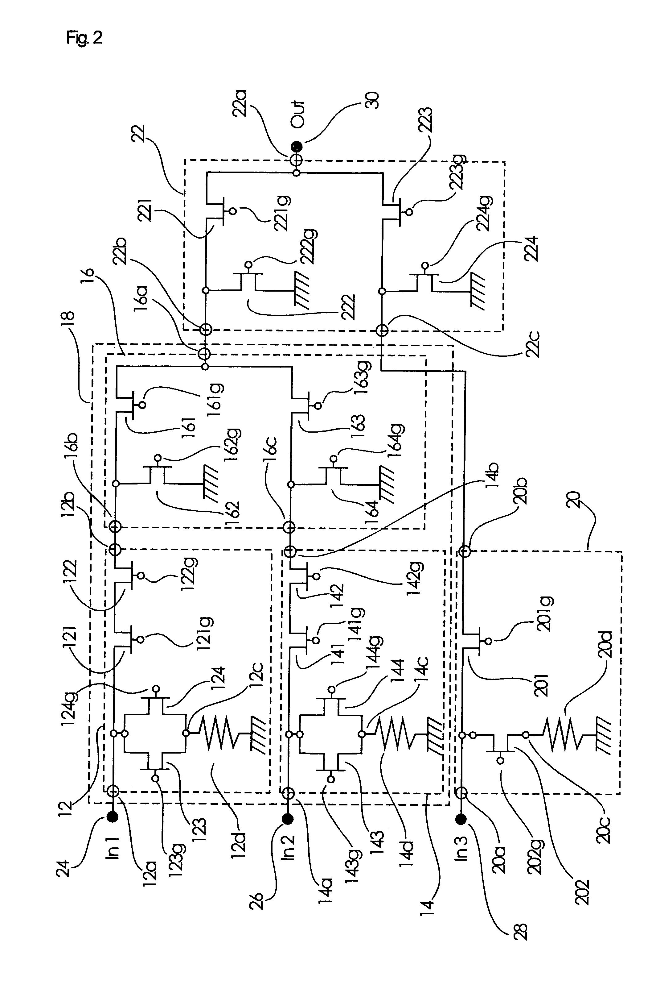
[0035]FIG. 1 is a block diagram showing a high frequency switch according to one embodiment of the present invention.

[0036]FIG. 1 describes an SP3T (1×3) type high frequency switch as one example.

[0037]In FIG. 1, the SP3T type high frequency switch 10 comprises an SPDT type high frequency switch 18 comprising an SPDT(A) 12 used as a first SPDT switch, an SPDT(B) 14 used as a second SPDT switch, and an SPDT(C) 16 used as a third SPDT switch, an SPDT(D) 20 used as a fourth SPDT switch and an SPDT(E) 22 used as a fifth SPDT switch in addition to the high frequency switch 18.

[0038]The SPDT(A) 12 has one pole 12a corresponding to a branch point, a first port 12b used as a first port and a second port 12c used as a second port both associated with one ends of paths branching off into two from the pole 12a. The pole 12a is connected to a first input terminal 24, and the second port 12c is grounded via a terminating resistor 12d.

[0039]The SPDT(B) 14 also has a first port 14b and a second p...

second embodiment

[0072]FIG. 5 is a block diagram showing a high frequency switch according to one embodiment of the present invention.

[0073]FIG. 5 describes an SP4T(1×4) type high frequency switch as one example.

[0074]In FIG. 5, the SP4T type high frequency switch 40 is further additionally provided with another SPDT type high frequency switch 48 comprising an SPDT(F) 42 used as a sixth SPDT switch, an SPDT(G) 44 used as a seventh SPDT switch and an SPDT(H) 46 used as an eighth SPDT switch in addition to an SPDT type high frequency switch 18 comprising an SPDT(A) 12 used as a first SPDT switch, an SPDT(B) 14 used as a second SPDT switch and an SPDT(C) 16 used as a third SPDT switch, and includes an SPDT(I) 50 used as a ninth SPDT switch.

[0075]The SPDT(F) 42 has a pole 42a, a first port 42b used as a first port and a second port 42c used as a second port both associated with one ends of paths branching off into two from the pole 42a. The pole 42a is connected to a third input terminal 52, and the sec...

third embodiment

[0106]FIG. 9 is a block diagram showing a high frequency switch according to one embodiment of the present invention.

[0107]FIG. 10 is a block diagram for describing the operation of the high frequency switch according to one embodiment of the present invention.

[0108]In FIG. 9, a 3×2 matrix switch 54 has a configuration in which the high frequency switch 10 according to the first embodiment is provided two side by side, and the first input terminals 24, the second input terminals 26 and the third input terminals 28 of the two high frequency switches 10 are respectively connected to one another. When the two high frequency switches 10 are used, the poles 12a of the SPDTs(A) 12, the poles 14a of the SPDTs(B) 14 and the poles 20a of the SPDTs(D) 20 are respectively connected to one another, and the number of input terminals is set to three and the number of output terminals is set to two.

[0109]Since the number of control terminals could be set to four without using the decoder in the hi...


PUM


Abstract

A high frequency switch device has SPDT(A), SPDT(B), and SPDT(C) switches, each having one pole and a first port and a second port, wherein the second port of the SPDT(A) is grounded via a terminating resistor and the second port of the SPDT(B) is grounded via a terminating resistor, respectively, and the first port of the SPDT(A) and the first port of the SPDT(B) are respectively connected to the first port and the second port of the SPDT(C).

Description

BACKGROUND OF THE INVENTION[0001]1. Field of the Invention[0002]The present invention relates to a high frequency switch device, and particularly to a high frequency switch device employed in a wireless communication apparatus, a satellite communication apparatus and a satellite broadcasting apparatus.[0003]2. Description of the related Art[0004]With a sudden proliferation of wireless communication apparatuses such as a cellular phone, a wireless LAN, etc. and more functionality or the like of information devices and systems due to a multichannel configuration of satellite broadcasting, there has recently been a sharp increase in demand for a high frequency switch employed in RF transmit-receive units of these devices and systems.[0005]The high frequency switch is used for switching between transmission and reception and switching between call modes in the case of a cellular phone and used for selection of signals from satellites of plural models in the case of a satellite dish. The...

Claims


Application Information

Patent Timeline
Patent Type & Authority Patents(United States)
IPC IPC(8): H01P1/10H01P1/15H03K17/00H03K17/693H04B1/18
CPCH03K17/693H01P1/15
Inventor KIZUKI, HIROTAKATANINO, NORIYUKISOMEI, JUNICHI
Owner MITSUBISHI ELECTRIC CORP
Why Eureka
Try Eureka