Method and apparatus for providing improved loop inductance of decoupling capacitors

a loop inductance and capacitor technology, applied in the field of decoupling capacitors, can solve the problems of increasing product cost, arguably ineffectiveness, and difficulty in maintaining the power source level applied to the integrated circuit (ic) within a prescribed range, and achieve the effect of improving the loop inductance of decoupling capacitors

Inactive Publication Date: 2007-12-25
GOOGLE LLC
View PDF13 Cites 11 Cited by
  • Summary
  • Abstract
  • Description
  • Claims
  • Application Information

AI Technical Summary

Benefits of technology

[0015]Another embodiment of the present invention is a method for providing improved loop inductance of decoupling capacitors. The method includes forming a first and second surface mount technology (SMT) mounting pad on a surface of a printed circuit board according to a predetermined arrangement, forming a first and second breakout via at one side of the SMT mounting pads and adjacent thereto, the first via being coupled to the first SMT mounting pad and a power plane and the second via being coupled to the second SMT mounting pad and to a ground plane, the forming of the first and second vias further comprising selecting a distance of separation between the first and second vias that is minimized according to allowable manufacturing tolerances and mounting a decoupling capacitor to the first and second SMT mounting pads at opposite ends.

Problems solved by technology

These and other achievements and increased levels of complexity has made it more and more difficult to maintain the power source level applied to an integrated circuit (IC) within a prescribed range.
This results in the need for more capacitors of differing values to accomplish a sufficiently low inductance, which adds to product cost and is arguably ineffective.
Decoupling problems are most acute for high performance printed circuit board designs, such as those with high speed logic, impedance controlled interconnect lines, and multiple voltage levels.
Problems arise from noise in the voltage supply planes adversely affecting logic chips and from return current discontinuities causing excessive coupling between signal lines.
However, the placement of the power and ground vias relative to the pads has never been minimized.
This results in input inductance that violate today's electrical requirements.

Method used


Image

  • Method and apparatus for providing improved loop inductance of decoupling capacitors
  • Method and apparatus for providing improved loop inductance of decoupling capacitors
  • Method and apparatus for providing improved loop inductance of decoupling capacitors

Examples


Embodiment Construction

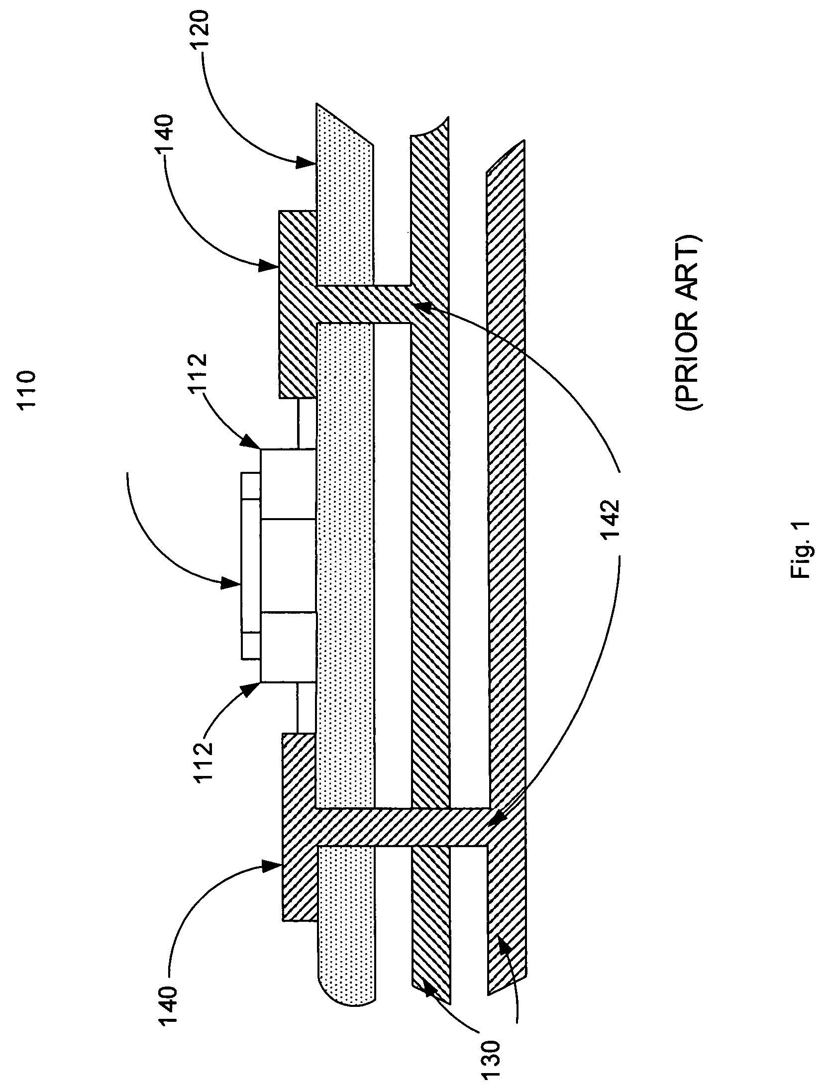
[0023]In the following description of the exemplary embodiment, reference is made to the accompanying drawings which form a part hereof, and in which is shown by way of illustration the specific embodiment in which the invention may be practiced. It is to be understood that other embodiments may be utilized as structural changes may be made without departing from the scope of the present invention.

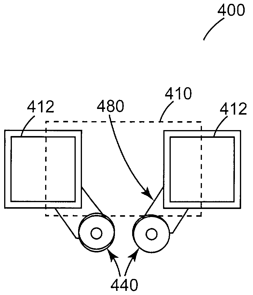
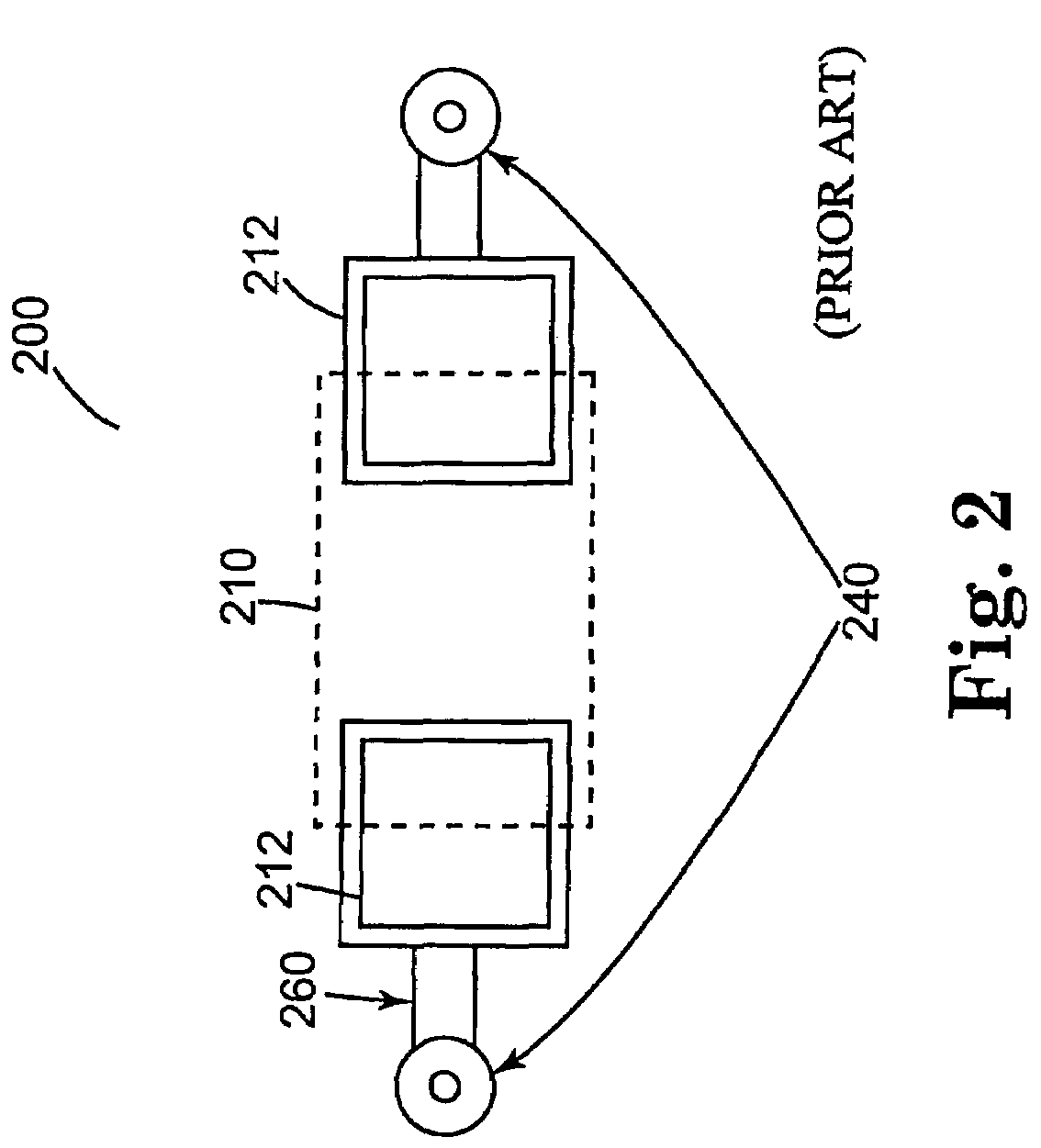
[0024]The present invention provides a method and apparatus that provides improved loop inductance of decoupling capacitors. Vias are moved close to the pads and close to each other. Instead of placing power and ground vias on opposite sides of the capacitor, these vias are moved around to the same side of the capacitor and are placed as close to each other as via-to-via manufacturing tolerances will allow.

[0025]For designs using standard two-terminal surface mount capacitors, two vias per capacitor, and standard manufacturing procedures (no vias inside pads, for example), the present inve...


PUM

PropertyMeasurementUnit
areasaaaaaaaaaa
loop inductanceaaaaaaaaaa
distanceaaaaaaaaaa

Abstract

A method and apparatus that provides improved loop inductance of decoupling capacitors. Vias are moved close to the pads and close to each other. Instead of placing power and ground vias on opposite sides of the capacitor, these vias are moved around to the same side of the capacitor and are placed as close to each other as manufacturing tolerances will allow. For designs using standard two-terminal surface mount capacitors, two vias per capacitor, and standard manufacturing procedures (no vias inside pads, for example), the lowest possible loop inductance of the capacitor's connections to the printed circuit board planes is provided. This results in the lowest effective capacitor series input inductance.

Description

BACKGROUND OF THE INVENTION[0001]1. Field of the Invention[0002]This invention relates in general to decoupling capacitors for integrated circuits, and more particularly to a method and apparatus for providing improved loop inductance of decoupling capacitors.[0003]2. Description of Related Art[0004]Recent developments in integrated circuit technologies have led to higher levels of performance and faster operation speeds and, also, have led to the development of more complex integrated circuits (ICs). These and other achievements and increased levels of complexity has made it more and more difficult to maintain the power source level applied to an integrated circuit (IC) within a prescribed range. For example, technological achievements in integrated circuit technologies have driven the operating frequencies (e.g., clocking speeds) to much higher levels and, correspondingly, are driving voltages as well as noise margins lower and lower.[0005]Surface mount capacitors are typically mo...

Claims


Application Information

Patent Timeline
Patent Type & Authority Patents(United States)
IPC IPC(8): H05K1/16H01K3/10H05K1/02H05K1/11
CPCH05K1/0231H05K1/114Y10T29/49165H05K2201/10636Y10T29/49133H05K2201/0792Y02P70/50
Inventor ANTU, RAFAELDREWS, CATHY MARIEPLOMGREN, DAVID A.TAKKEN, TODD EDWARD
Owner GOOGLE LLC
Why Eureka
Try Eureka