
Static random access memory (SRAM) bit cell circuits with a minimum distance between a storage circuit active region and a read port circuit active region to reduce area and SRAM bit cell array circuits

a technology of random access memory and bit cell array circuits, which is applied in the field of memory circuits to reduce the area of memory circuits, and achieves the effect of reducing the area

Active Publication Date: 2022-03-29
QUALCOMM INC
View PDF9 Cites 0 Cited by
  • Summary
  • Abstract
  • Description
  • Claims
  • Application Information

AI Technical Summary

Benefits of technology

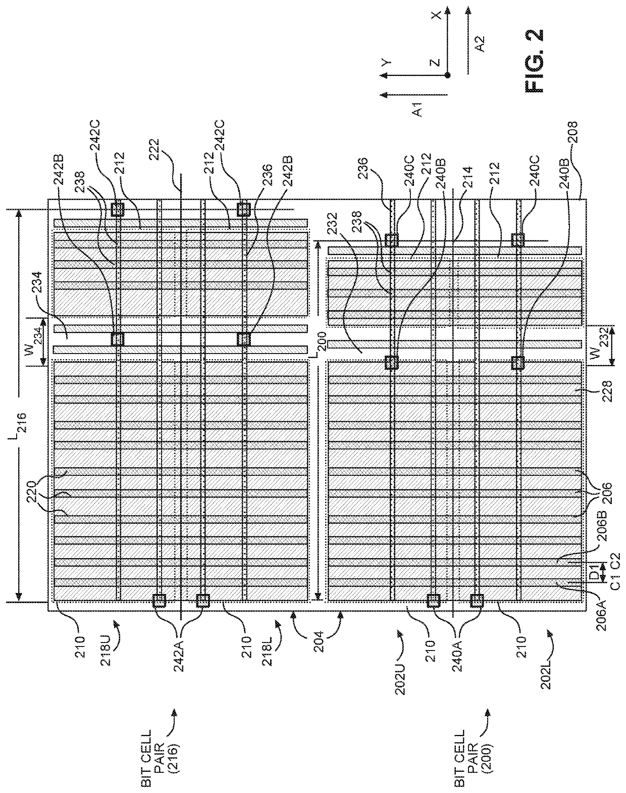
The SRAM bit cell described in this patent has a smaller size because the distance between the active areas of the storage circuit and the read port is reduced. By minimizing this distance, the area of the cell is minimized. This is achieved by relocating the gate contact of a write access transistor from a location between the two areas to a location overlapping the storage circuit area. This reduces the separation distance and allows for a smaller cell size.

Problems solved by technology

In some examples, a processing circuit can issue more than one read operation to an SRAM array, which can cause conflicts between overlapping read operations.

Method used


Image

  • Static random access memory (SRAM) bit cell circuits with a minimum distance between a storage circuit active region and a read port circuit active region to reduce area and SRAM bit cell array circuits
  • Static random access memory (SRAM) bit cell circuits with a minimum distance between a storage circuit active region and a read port circuit active region to reduce area and SRAM bit cell array circuits
  • Static random access memory (SRAM) bit cell circuits with a minimum distance between a storage circuit active region and a read port circuit active region to reduce area and SRAM bit cell array circuits

Examples


Embodiment Construction

[0019]With reference now to the drawing figures, several exemplary aspects of the present disclosure are described. The word “exemplary” is used herein to mean “serving as an example, instance, or illustration.” Any aspect described herein as “exemplary” is not necessarily to be construed as preferred or advantageous over other aspects.

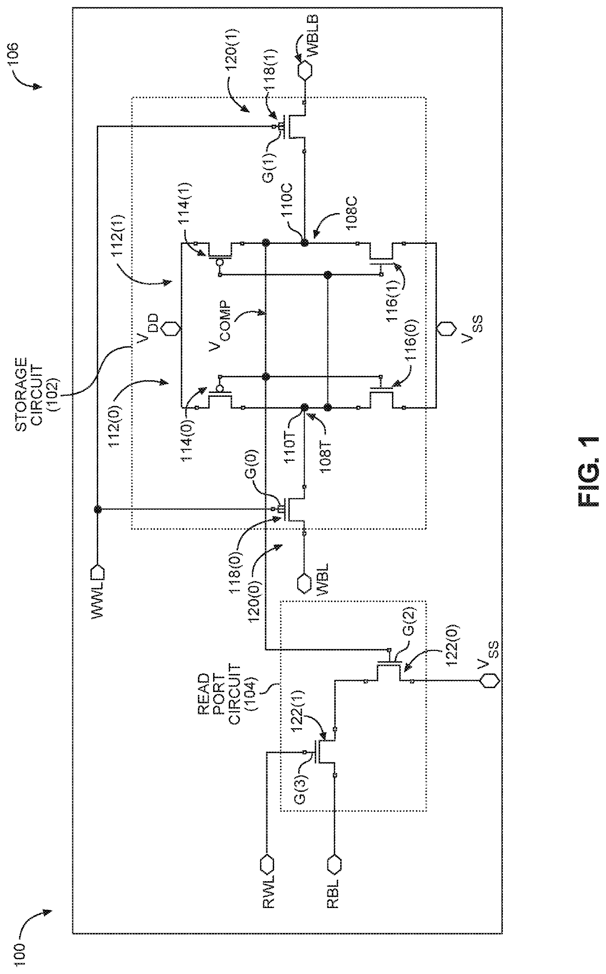
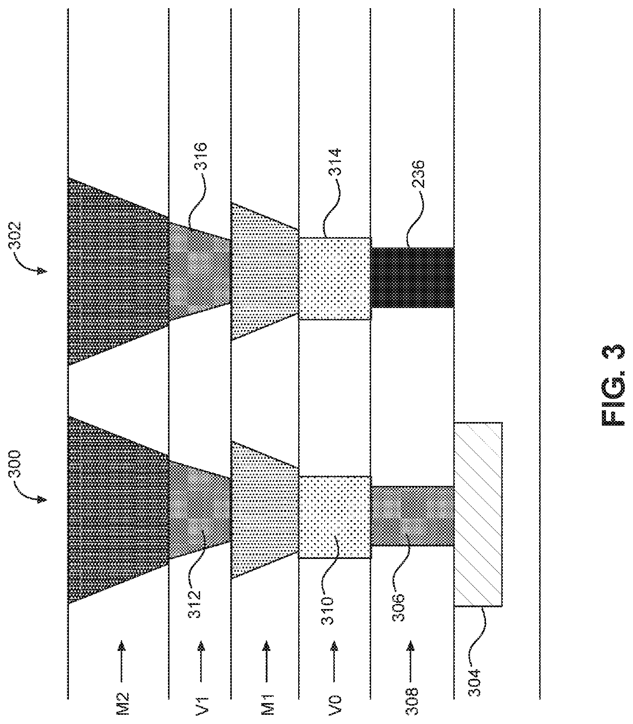
[0020]Aspects disclosed herein include static random access memory (SRAM) cell circuits with a minimum distance between a storage circuit active region and a read port circuit active region to reduce area. SRAM bit cell array circuits and related fabrication methods are also disclosed. SRAM bit cells are implemented as complementary metal oxide semiconductor (CMOS) circuits. Transistors of the CMOS circuits are provided as Fin Field-Effect Transistors (FETs) (Fin-FETs) formed in fins on a substrate, and an array of fins can be used to create an SRAM bit cell array circuit. Each SRAM bit cell circuit (“SRAM bit cell”) in an SRAM bit cell array circuit ...


PUM


Abstract

SRAM cell circuits have a minimum distance between a storage circuit active region and a read port circuit active region to reduce area. SRAM cell circuits are formed in FinFETs in a storage circuit active area and a read port active area each including one or more diffusion regions of a substrate. Design rule constraints limit a minimum center-to-center distance between adjacent parallel fins. The SRAM bit cell has a reduced total area because a distance between the storage circuit active area and the read port active area is reduced to a minimum separation distance of between 1.0 and 2.15 times the smallest center-to-center distance between adjacent fins. Minimizing a separation distance may include relocating a gate contact of a write access transistor from a location between the storage circuit active region and the read port active region to a location overlapping the storage circuit active area.

Description

BACKGROUNDI. Field of the Disclosure[0001]The field of the disclosure relates generally to memory circuits in an integrated circuit and, more particularly, to reducing the area of memory circuits.II. Background[0002]Integrated circuit (IC) chips with processing circuits are indispensable to the functionalities of electronic devices. Processing circuits (“processors”) read instructions and data from memory circuits for processing and store the processed data back into the memory circuits. Static random access memory (SRAM) is a type of memory circuit that can be employed in processors. SRAM contains a plurality of bit cells organized in rows and columns of an SRAM bit cell array in which each bit cell can store a single data value (bit) of digital data. Each bit cell includes a storage circuit and at least one access port for accessing the storage circuit. Accessing the storage circuit includes writing a data value into the storage circuit in response to a write operation and reading...

Claims


Application Information

Patent Timeline
Patent Type & Authority Patents(United States)
IPC IPC(8): H01L27/11G11C11/419H01L23/522H01L21/8238H01L27/092
CPCH01L27/1104G11C11/419H01L21/823821H01L23/5226H01L27/0924H01L27/1116G11C11/412H01L27/0207H10B10/18H10B10/12
Inventor BIRADAR, RAHULSHARMA, SUNILDESAI, CHANNAPPAGHOSH, SONIA
Owner QUALCOMM INC
Learn More