Structure with embedded opto-electric components

a technology of opto-electric components and structures, applied in the direction of optical elements, circuit optical details, instruments, etc., can solve the problems of difficult fabrication of semiconductors with higher performance, delay in signal time, and difficulty in efficiently dispersing heat, so as to reduce photo beam loss, improve transmission quality, and compact size

Active Publication Date: 2007-12-25
PHOENIX PRECISION TECH CORP
View PDF2 Cites 6 Cited by
  • Summary
  • Abstract
  • Description
  • Claims
  • Application Information

AI Technical Summary

Benefits of technology

[0018]In light of the above drawbacks in the conventional technology, an objective of the present invention is to provide a structure with embedded opto-electric components, which can reduce loss of a photo beam during a transmission process.
[0019]Another objective of the present invention is to provide a structure with embedded opto-electric components, which can modularize optical / electronic conversion.
[0020]Still another objective of the present invention is to provide a structure with embedded opto-electric components, so as to prevent occupation of space and reduce a volume of the structure.

Problems solved by technology

However, in the case of a data transmission rate reaching a degree of Gb / s, several drawbacks are caused such as difficulty in efficiently dissipating heat, delay of signal time, electromagnetic interference, and so on, making fabrication of a semiconductor with higher performance become difficult.
In particular for conventionally using copper circuits as data signal transmission media, conductivity of the copper circuits is hardly improved due to a limitation of the material characteristic thereof, such that the speed of signal transmission cannot be enhanced by a try to improve the conductivity.
For a structure using metal circuits to transmit signals, it is easily affected by interference from external noise or interference between internal circuits during a signal transmission process, thereby causing errors in signal transmission due to the interference.
However, such protective mechanism leads to considerable difficulty in a circuit design and requires an additional structural design, making the design and fabrication costs undesirably increased and thereby not effective to solve the problem in the current situation.
However, the current signal processing method within circuits is mostly by digital processing, and signal conversion during the signal transmission process easily causes distortion and errors in data transmission after the signal conversion.
However, this technology is not favorable for the design of having a compact size and a small profile due to a requirement of high precision of optical alignment and a large system volume.
However, a drawback caused by the above conventional structure is that, it is difficult to form the pair of 45-degree reflection surfaces 22a, 22b at the two terminals of the waveguide 22.
The above conventional structure also requires high precision of optical alignment and thus increases the fabrication costs thereof.
Further, since the photo beam must undergo two reflections via the reflection surfaces 22a, 22b, it may cause relatively greater loss of optical signals.
However, this arrangement increases the overall thickness of the structure by using the elevated circuit boards 23′ and similarly leads to the area occupying drawback, such that the requirement of having a compact size and a small profile cannot be satisfied for the structure.
Thus, the assembly costs and difficulty in fabrication control of the structure are increased, thereby raising the fabrication costs.
Moreover, there is no heat dissipating structure provided for the optical active component 24 and the optical receiving component 25, such that the overall heat dissipating effect is not satisfactory, and the optical active component 24 and the optical receiving component 25 may easily be damaged by overheating.

Method used


Image

  • Structure with embedded opto-electric components
  • Structure with embedded opto-electric components
  • Structure with embedded opto-electric components

Examples


Embodiment Construction

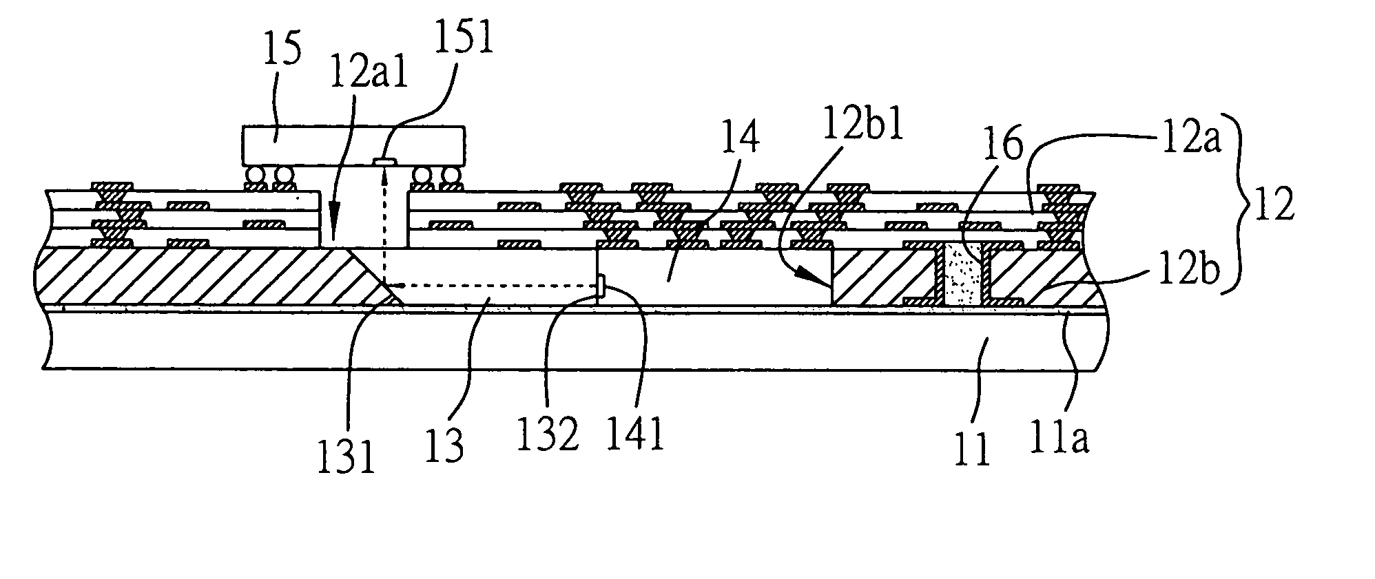
[0039]Preferred embodiments of a structure with embedded opto-electric components proposed in the present invention are described as follows with reference to FIGS. 3A-3C, 4 and 5.

[0040]FIGS. 3A to 3C are cross-sectional schematic diagrams of the structure with embedded opto-electric components according to the present invention. As shown in FIGS. 3A to 3C, the structure with embedded opto-electric components comprises: a carrier 11, which may be a metallic plate, a ceramic plate, or an organic substrate such as a printed circuit board or an IC (integrated circuit) package substrate; at least one circuit board 12 mounted on the carrier 11, and comprising an upper board 12a (e.g. a printed circuit board or an IC package substrate) and a lower board 12b (e.g. an insulating board), wherein the upper board 12a has a cavity 12a1, and the lower board 12b has a receiving space 12b1 communicating with the cavity 12a1 of the upper board 12a; at least one waveguide 13 mounted on the carrier 1...


PUM


Abstract

A structure with embedded opto-electric components includes a carrier; at least one circuit board having a cavity and mounted on a carrier; at least one waveguide embedded in an inner layer of the circuit board and mounted on the carrier; at least one first opto-electric component embedded in the inner layer of the circuit board, and having an active terminal in contact with a transmission terminal of the waveguide; and at least one second opto-electric component mounted on the circuit board, and having an active terminal corresponding in position to another transmission terminal of the waveguide via the cavity. Since the first opto-electric component and the waveguide are in contact with each other and embedded in the circuit board, an optical transmission mechanism is simplified and times of reflection are decreased, thereby reducing errors and loss during transmission.

Description

FIELD OF THE INVENTION[0001]The present invention relates to structures with embedded opto-electric components, and more particularly, to a structure for fixing and embedding opto-electric components in a carrier.BACKGROUND OF THE INVENTION[0002]Along with continuous development of the semiconductor technology, semiconductor packages are required to not only have a compact size and a small profile but also have enlarged capacity for data storage. In light of increase in a load of data to be processed, relatively higher processing efficiency is achieved by processing data of the same size in a faster speed. The most direct way to enhance the processing speed of a semiconductor is to increase a frequency used by the semiconductor. However, in the case of a data transmission rate reaching a degree of Gb / s, several drawbacks are caused such as difficulty in efficiently dissipating heat, delay of signal time, electromagnetic interference, and so on, making fabrication of a semiconductor ...

Claims


Application Information

Patent Timeline
Patent Type & Authority Patents(United States)
IPC IPC(8): G02B6/12
CPCG02B6/12002G02B6/12004G02B6/4214H05K1/0274G02B6/43H05K2201/09536H05K1/185H05K3/4602H01L2224/16225
Inventor HSU, SHIH-PING
Owner PHOENIX PRECISION TECH CORP
Why Eureka
Try Eureka