Semiconductor memory device having resistor and method of fabricating the same

a memory device and resistor technology, applied in the direction of resistors, solid-state devices, basic electric elements, etc., can solve the problems of abnormal operation of the dram device, difficult to maintain uniform uneven width of the resistor, so as to increase the cost of patterning and uniform width.

Inactive Publication Date: 2008-01-15
SAMSUNG ELECTRONICS CO LTD
View PDF28 Cites 12 Cited by
  • Summary
  • Abstract
  • Description
  • Claims
  • Application Information

AI Technical Summary

Benefits of technology

[0007]It is an object of the present invention to provide a method for forming a semiconductor device, wherein resistors on the peripheral circuit area have substantially uniform widths without substantially increasing the cost for patterning the plate node layer.
[0008]It is another object of the present invention to provide a method for forming a DRAM device, wherein resistors on the peripheral circuit area have substantially uniform resistance values without substantially increasing the cost for patterning the plate node layer.
[0009]It is another object of the present invention to provide a semiconductor device, wherein resistors on the peripheral circuit area have substantially uniform widths and resistance values so as to substantially avoid abnormal operations of the semiconductor device.
[0011]According to another aspect of the present invention, a method of fabricating a semiconductor device is provided. The method comprises providing a substrate and defining a first area and a second area in the substrate. A mold layer is formed on the substrate and in the first and second areas. An anti-reflective layer is formed on the mold layer. A first portion of the anti-reflective layer is selectively etched, thereby reducing the thickness of the anti-reflective layer in the first area. The first portion of the anti-reflective layer is located in the first area. First molding holes and a second molding hole are formed in the first area and second area respectively by patterning the mold layer and the anti-reflective layer. A second portion of the anti-reflective layer is etched to leave a remaining portion of the anti-reflective layer only in the second area. A storage node layer is formed on the mold layer as well as in the first and second molding holes. A plurality of storage nodes and a first portion of a resistor are formed in the first molding holes and in the second molding hole respectively by removing a portion of the storage node layer. The first portion of a resistor is formed of the storage node layer. Each of the storage nodes has an inner wall and an outside wall. A portion of the mold layer is etched by using the remaining portion of the anti-reflective layer as a etch mask, thereby exposing a portion of the outside wall and leaving a remaining portion of the mold layer in the second area. A portion of the mold layer is located in the first area. The remaining portion of the mold layer has the second molding hole therethrough.

Problems solved by technology

However, in recent DRAM devices having high packing density, the patterns of the resistors are not fine.
That is, it is very difficult to maintain uniformity in the widths of the resistors.
As a result, abnormal operations of the DRAM devices may occur.
The width irregularity problem is mainly due to the above-mentioned step difference between the cell array area and the peripheral circuit area.
However, the cost of the advanced process is too expensive such that it cannot be widely accepted in industry.

Method used


Image

  • Semiconductor memory device having resistor and method of fabricating the same
  • Semiconductor memory device having resistor and method of fabricating the same
  • Semiconductor memory device having resistor and method of fabricating the same

Examples


first modified embodiment

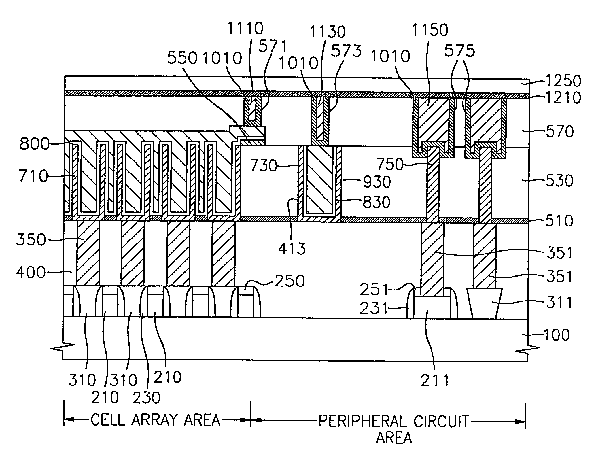
[0030]In the present invention, the width of the second molding hole 413 is so narrow enough that the storage node layer 700 completely fills the second molding hole 413. In this case, the capacitor dielectric layer 800 and the plate node layer 900 are not formed in the second molding hole 413, but formed on the first portion 730 of the resistor.

second modified embodiment

[0031]In the present invention, the widths of the third molding holes 415 are wide enough that the storage node layer 700 does not completely fill the third molding holes 415, but is conformably formed on the bottoms and sidewalls as with the first molding holes 411. In this case, the capacitor dielectric layer 800 and / or the plate node layer 900 may be formed in the third molding holes 415.

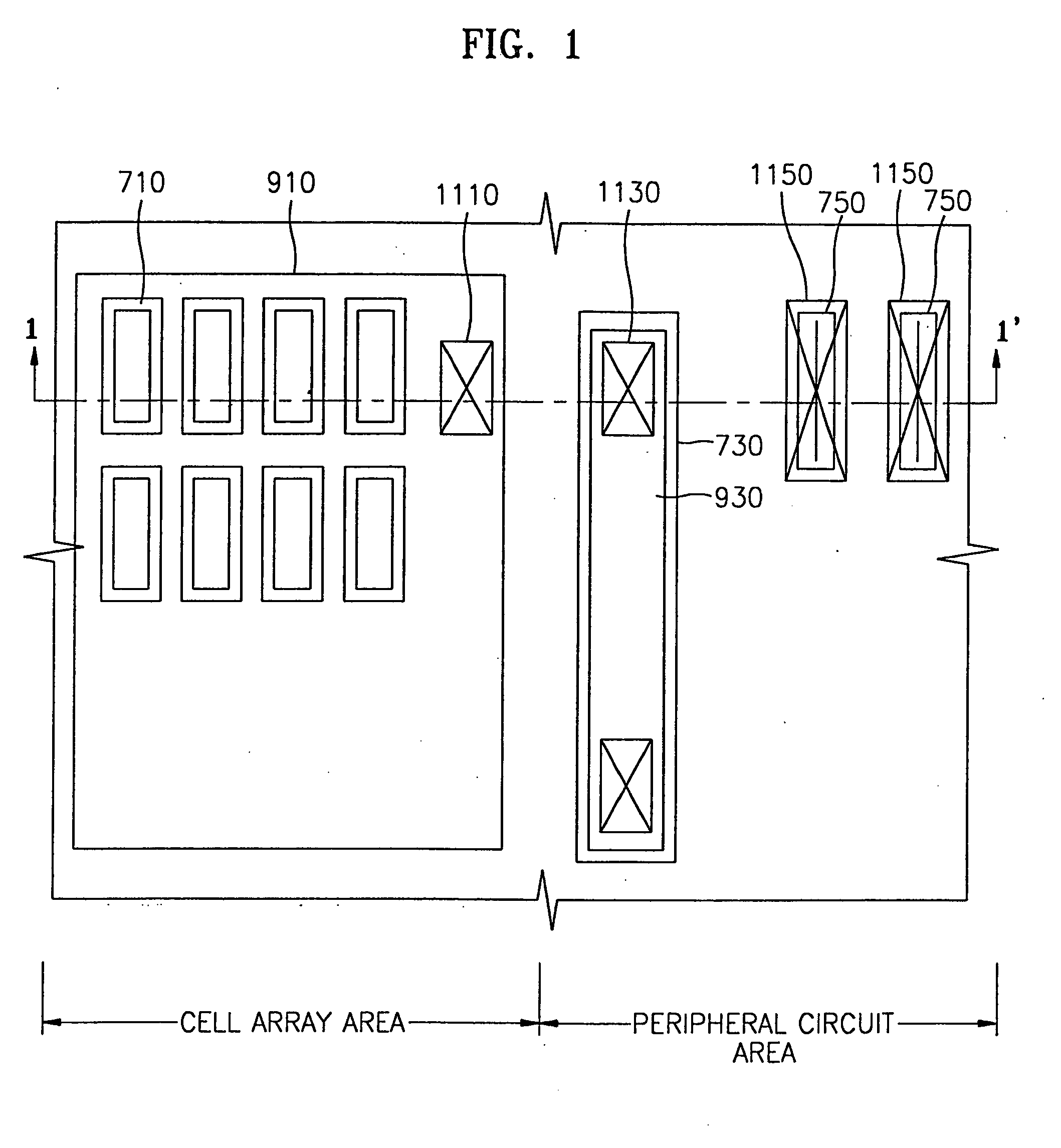
[0032]Referring to FIGS. 1 and 9, the plate node layer 900 and the capacitor dielectric layer 800 are patterned by a photolithography technique to form a plate node 910 on the plurality of storage nodes 710 in the cell array area. Moreover, the plate node layer 900, the capacitor dielectric layer 800 and the anti-reflective layer 550 are removed simultaneously in a portion of the peripheral circuit area except in the second molding hole 413. As a result, the remaining portion of the mold layer 530 is exposed and a second portion 830 of the resistor in the second molding hole 413 and a third porti...


PUM

PropertyMeasurementUnit
capacitanceaaaaaaaaaa
heightaaaaaaaaaa
heightaaaaaaaaaa

Abstract

A semiconductor device having resistors in a peripheral area and fabrication method thereof are provided. A mold layer is formed on a semiconductor substrate. The mold layer is patterned to form first molding holes and a second molding hole in the mold layer. A storage node layer is formed on the mold layer as well as in the first and second molding holes. The storage node layer is patterned to form storage nodes in the first molding holes and a portion of a resistor in the second hole.

Description

[0001]This application is a divisional of U.S. Pat. No. 10 / 272,670, filed on Oct. 16, 2002 now U.S. Pat. No. 6,794,247, now pending, which is herein incorporated by reference in its entirety.FIELD OF THE INVENTION[0002]The present invention relates to a semiconductor device and method of fabricating the same, and more specifically to a dynamic random access memory (DRAM) device having a resistor and method of fabricating the same.BACKGROUND OF THE INVENTION[0003]Generally, a DRAM device comprises a cell array area and a peripheral circuit area. The cell array area includes a plurality of unit cells, each of which comprises a MOS transistor and a storage capacitor. The storage capacitor comprises a lower electrode (i.e., storage node) and an upper electrode (i.e., plate node). It is a generally accepted fact in industry that the capacitance of the storage capacitor is required to be 0.25 μF or more, while the unit cell size has been constantly reduced for higher packing density of a ...

Claims


Application Information

Patent Timeline
Patent Type & Authority Patents(United States)
IPC IPC(8): H01L27/108H01L29/76H01L29/94H01L31/0392H01L31/119H01L21/108H01L21/8242H01L27/06H01L27/105
CPCH01L27/0629H01L27/105H01L27/10894H01L27/10814H01L27/10882Y10S257/904H10B12/315H10B12/48H10B12/09H01L21/108
Inventor KWAK, DONG-HWAKIM, BYUNG-SEO
Owner SAMSUNG ELECTRONICS CO LTD
Why Eureka
Try Eureka