Multi-layer structure for use in the fabrication of integrated circuit devices and methods for fabrication of same

Inactive Publication Date: 2008-01-22
LOCKHEED MARTIN CORP +1
View PDF19 Cites 90 Cited by
  • Summary
  • Abstract
  • Description
  • Claims
  • Application Information

AI Technical Summary

Problems solved by technology

However, a power HEMT or pHEMT, unlike a conventional depletion mode HEMT or PHEMT, typically requires a double gate recess, having two aligned recesses of different widths.

Method used


Image

  • Multi-layer structure for use in the fabrication of integrated circuit devices and methods for fabrication of same
  • Multi-layer structure for use in the fabrication of integrated circuit devices and methods for fabrication of same
  • Multi-layer structure for use in the fabrication of integrated circuit devices and methods for fabrication of same

Examples


Embodiment Construction

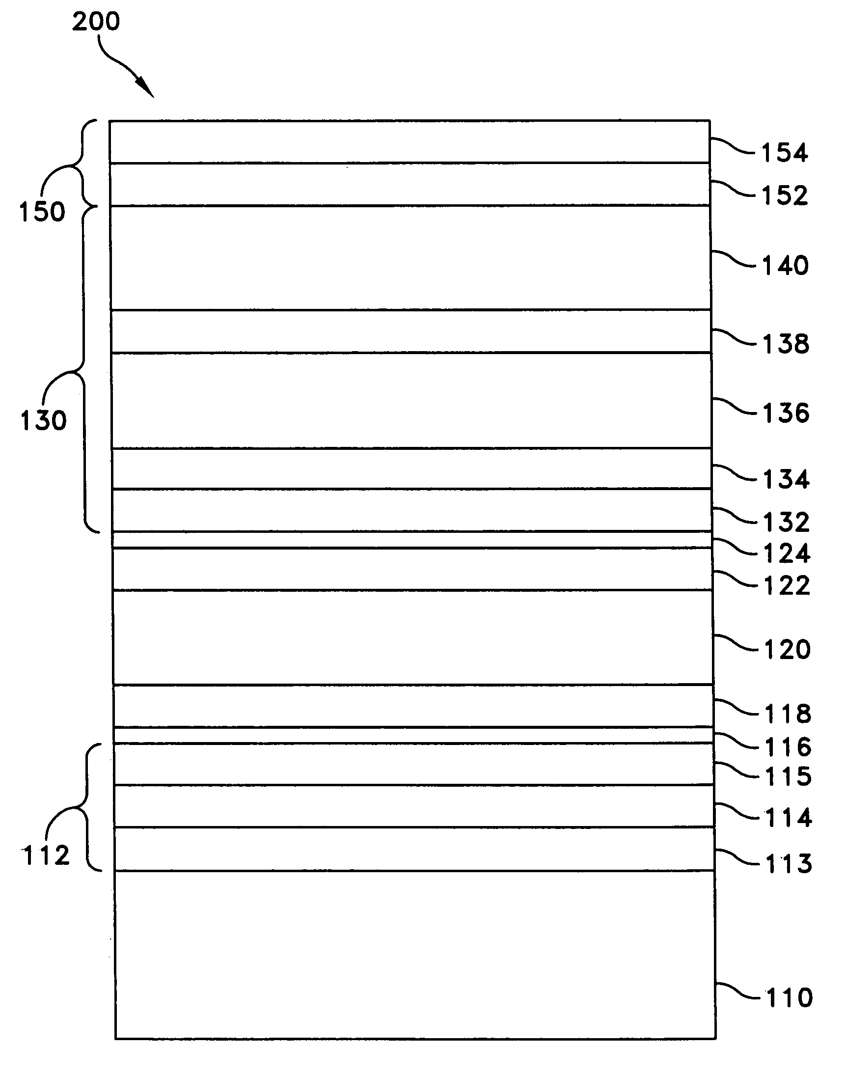
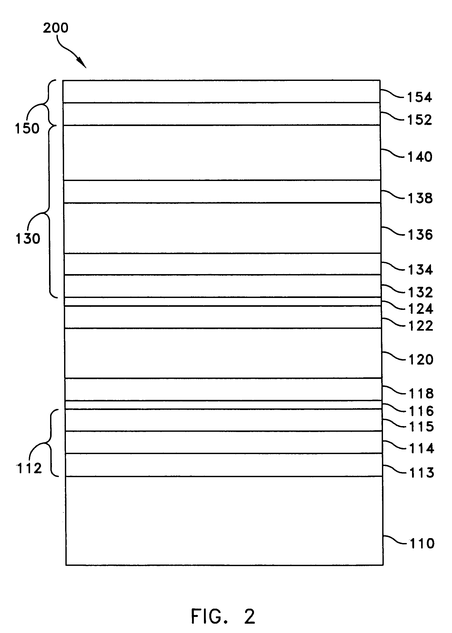
[0022]Referring to FIG. 2 a multi-layer structure according to an embodiment of the invention will now be described. Structure 200 is a multi-layer structure adapted for formation of three different types of devices, and in particular three different types of HEMTs, and in particular three different types of pHEMTs, which types are characterized by at least two different pinch-off voltages.

[0023]The multi-layer structure 200 has a substrate 110. Substrate 110 may be of a semi-insulating material, such as GaAs. Buffer layer 112 is formed on substrate 110. Buffer layer 112 may include a superlattice layer 113, an undoped AlAs layer 114 on superlattice layer 113, and an undoped AlGaAs layer 115 on undoped AlAs layer 114. A superlattice is a semiconductor structure having at least four, and typically many more, extremely thin layers of semiconductor material, generally not more than about 100 angstroms each, and in some implementations not more than about 40 angstroms each; adjacent lay...


PUM


Abstract

A multi-layer structure for use in the fabrication of integrated circuit devices is adapted for the formation of enhancement mode high electron mobility transistors, depletion mode high electron mobility transistors, and power high electron mobility transistors. The structure has, on a substrate, a channel layer, spacer layer on the channel layer, a first Schottky layer, a second Schottky layer on the first Schottky layer, and a third Schottky layer on the second Schottky layer, and a contact layer on the third Schottky layer. Etch stops are defined intermediate the first and second Schottky layers, intermediate the second and third Schottky layers, and intermediate the third Schottky layer and the contact layer.

Description

FIELD OF INVENTION[0001]The present invention relates to integrated circuit devices, and more particularly to active layers for use in the fabrication of integrated circuit devices, particularly high electron mobility transistors.BACKGROUND[0002]Several types of field effect transistors (FETs) are available for use at microwave and millimeter wave frequencies in the fabrication of monolithic microwave integrated circuits (MMIC). FETs that operate at these frequencies are generally referred to as high-frequency FETs. These high frequency FETs include metal semiconductor field effect transistors (MESFETs) and high electron mobility transistors (HEMTs). Typically, HEMTs are formed from Group III-V materials such as gallium arsenide (GaAs) or indium phosphide (InP), although other materials may be used. In a HEMT there is a doped donor / undoped spacer layer of one material and an undoped channel layer of a different material. A heterojunction is formed between the doped donor / undoped spa...

Claims


Application Information

Patent Timeline
Patent Type & Authority Patents(United States)
IPC IPC(8): H01L29/06H01L21/338H01L29/201H01L29/732
CPCH01L29/66462H01L29/7785
Inventor ROBINSON, KEVIN L.WITKOWSKI, LARRYKAO, MING-YIH
Owner LOCKHEED MARTIN CORP
Why Eureka
Try Eureka