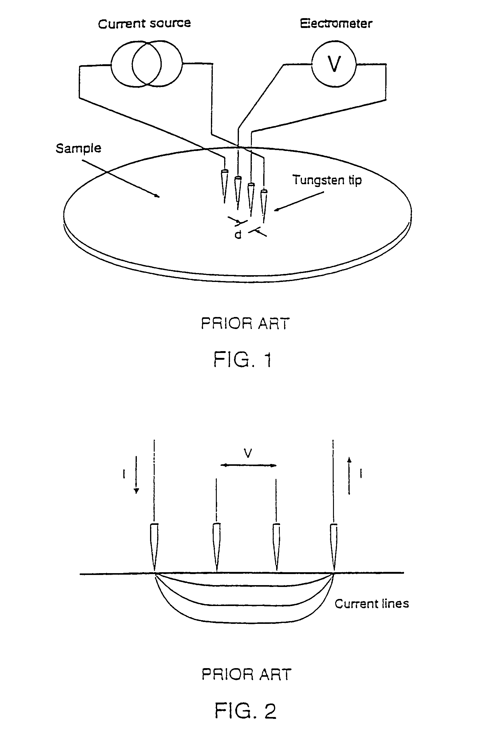
Multi-point probe

a multi-point probe and probe body technology, applied in the direction of individual semiconductor device testing, semiconductor/solid-state device testing/measurement, instruments, etc., can solve the problems of one tip with inferior physical contact, and no technology is currently available to obtain the electric properties of individual devices on semiconductor wafers

Inactive Publication Date: 2008-01-29
CAPRES
View PDF25 Cites 43 Cited by
  • Summary
  • Abstract
  • Description
  • Claims
  • Application Information

AI Technical Summary

Benefits of technology

[0011]A particular advantage of the present invention is related to the fact that the novel testing technique involving a novel multi-point probe allows the probe to be utilised for establishing a reliable contact between any testing pin or testing tip and a specific location of the test sample, as the testing probe according to the present invention includes individually bendable or flexible probe arms.
[0012]A particular feature of the present invention relates to the fact that the testing probe according to the present invention may be produced in a process compatible with the production of electronic circuits, allowing measurement electronics to be integrated on the testing probe, and allowing for tests to be performed on any device fabricated by any appropriate circuit technology involving planar technique, CMOS technique, thick-film technique or thin-film technique and also LSI and VLSI production techniques.
[0013]The above object, the above advantage and the above feature together with numerous other objects, advantages and features which will be evident from the below detailed description of a preferred embodiment of the present invention is according to a first aspect of the present invention obtained by a multi-point probe for testing electric properties on a specific location of a test sample, comprising:
[0015](b) a first multitude of conductive probe arms positioned in co-planar relationship with surface of said supporting body, and freely extending from said supporting body, giving individually flexible motion of said first multitude of conductive probe arms; and
[0016](c) said conducting probe arms originating from a process of producing said multi-point probe including producing said conductive probe arms on supporting wafer body in facial contact with said supporting wafer body and removal of a part of said wafer body providing said supporting body and providing said conductive probe arms freely extending from said supporting body.
[0017]According to the basic realisation of the present invention, the multi-point probe according to the first aspect of the present invention is implemented in accordance with the technique of producing electronic circuits, in particular involving planar techniques as the probe is produced from a supporting body, originating from a wafer body on which a first multitude of conductive probe arms are produced involving deposition, accomplished by any technique known in the art, such as chemical vapour deposition (CVD), plasma enhanced CVD (PECVD), electron cyclotron resonance (ECR) or sputtering, etching or any other production technique, for example high resolution lithographic methods such as electron-beam lithography, atomic force microscopy (AFM) lithography or laser lithography, whereupon a part of the original supporting body is removed through mechanical grinding or etching producing the freely extending conducting probe arms characteristic to the present invention constituting the test pins of multi-point probes according to the first aspect of the present invention.

Problems solved by technology

However, since the tips are situated on the same cantilever beam the pressure monitored while monitoring the maximum pressure may possibly leave one tip with an inferior physical contact.
Furthermore, apart from the above described limitations as to establishing contact with the surface of the test sample to be tested the prior art probes possess limitations as to miniaturisation of the testing technique as the probes hitherto known limit the maximum spacing between any two tips to a dimension in the order of 0.5 mm due to the production technique involving mechanical positioning and arresting of the individual testing pins or testing tips, in particular as far as the four-point probes are concerned, and as far as the SR-probes are concerned exhibit extreme complexity as far as the overall structure is concerned and also certain drawbacks as far as the utilisation of the SR-probe due to the overall structure of the SR-probe.
It appears that no technique is currently available for obtaining the electric properties of individual devices on semiconductor wafers, without possible destruction of device junctions.

Method used


Image

  • Multi-point probe
  • Multi-point probe
  • Multi-point probe

Examples


Embodiment Construction

[0091]A preferred embodiment is directed toward making a multi-point probe and is described with respect to FIGS. 3-6.

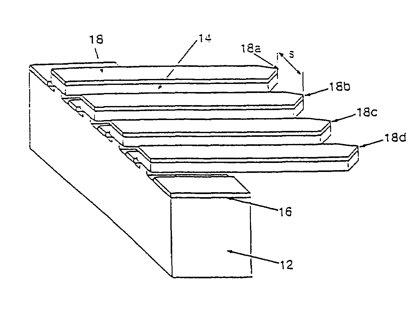
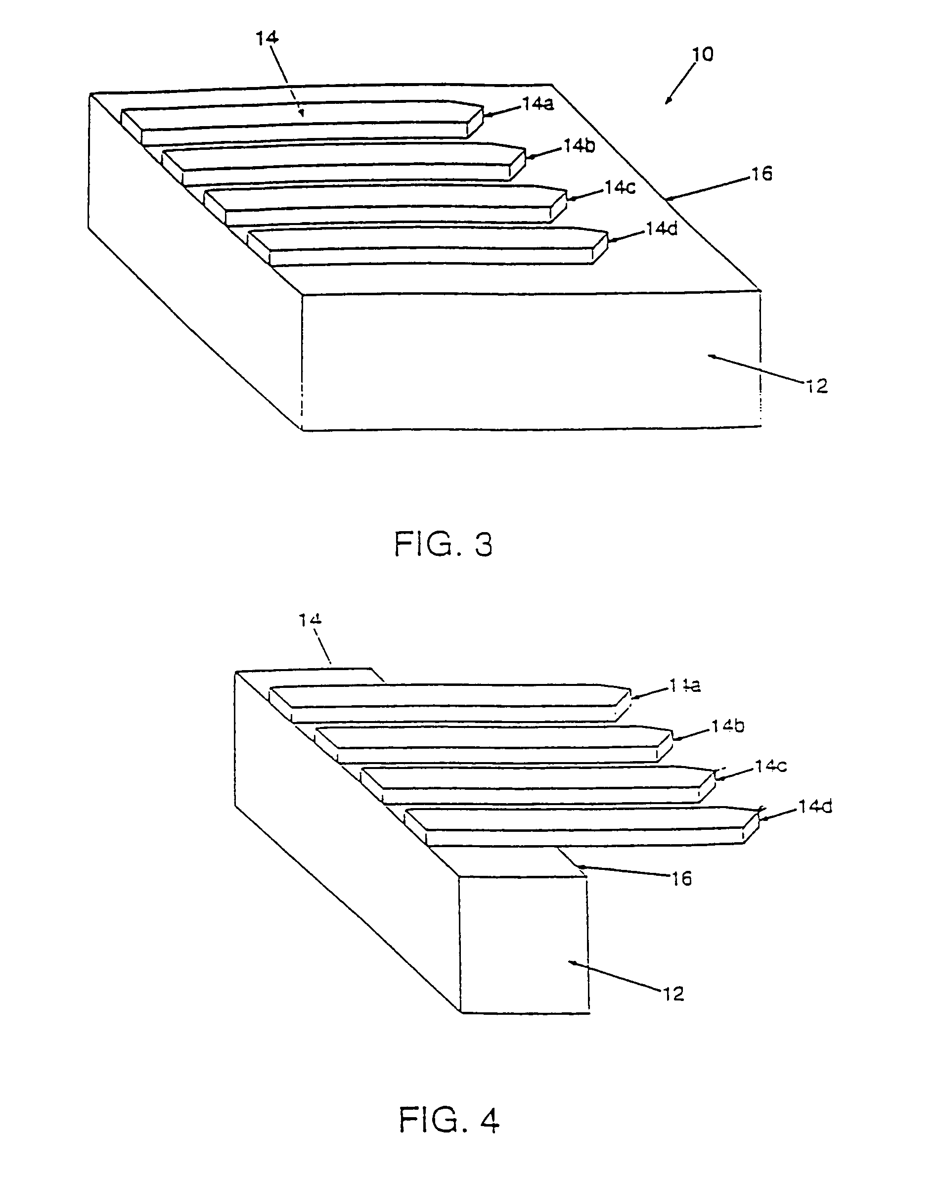
[0092]FIG. 3 shows a wafer 10, for example a section of a semiconductor wafer, in intermediate state of fabrication. It shows a surface 16 of a substrate 12 covered by a support layer 14, being electrically isolating, such as silicon oxide. The deposition of the support layer 14 can be accomplished by any technique known in the art, such as chemical vapour deposition (CVD), plasma enhanced CVD (PECVD), electron cyclotron resonance (ECR) or sputtering. As shown in FIG. 3, the support layer 14 is patterned and etched to form beams with tapered end-points 14a-d. The beams are not limited to any particular form or symmetry; they can be of any geometry with suitable end-points.

[0093]The pattern is formed by forming a photoresist pattern (not shown in FIG. 3) which defines the four beams on the top surface of the support layer 14. The photoresist pattern is formed by conve...


PUM


Abstract

A multi-point electrical probe for testing location-specific electrical properties on circuit boards. Four generally parallel, electrically conducting probe arms are produced preferably by wafer-based techniques, although any even number of probe arms between two and 64 may be used. The precision of wafer-based manufacturing techniques permits miniaturization beyond that which is conventionally obtained by assembling discrete components. The probe arms are generally flexible, and may be shaped suitably to accommodate a particular circuit geometry. The probe and / or the sample under test may be precisely located by suitable translation and / or rotation stages, which may optionally be placed under computer control. A suitable wiring diagram is provided, and preferable manufacturing techniques are discussed. In addition, the conducting probe arms benefit from active guarding, which reduces leakage resistance and increases the measuring accuracy of the probe, by the inclusion of electrically-isolated conducting regions located between the probe arms.

Description

CROSS-REFERENCE TO RELATED APPLICATION[0001]The present application is a continuation of U.S. application Ser. No. 09 / 750,645 filed Dec. 28, 2000, now abandoned, which is a continuation of PCT / DK99 / 00391, filed Jul. 8, 1999, which is incorporated herein by reference thereto in its entirety, as though fully set forth therein.FIELD OF THE INVENTION[0002]The present invention generally relates to the technique of testing electric properties on a specific location of a test sample and in particular the technique of probing and analysing semiconductor integrated circuits for example of LSI and VLSI complexity.DESCRIPTION OF THE RELATED ART[0003]The most commonly used technique of testing the electric properties of a test sample involves the generation of resistivity or carrier concentration profiles of the surface of a processed semiconductor wafer by the utilisation of a four-point probe as described in published international patent application WO 94 / 11745. Furthermore, see for example...

Claims


Application Information

Patent Timeline
Patent Type & Authority Patents(United States)
IPC IPC(8): G01R31/02G01R1/073G01R1/06G01R1/067G01R27/02G01R27/04G01R27/14G01R31/26G01R31/28H01L21/66
CPCG01R1/06733G01R1/07307G01R27/14G01R1/06711G01R1/06755G01R27/04G01R31/2648G01R31/2831G01R1/06727
Inventor PETERSEN, CHRISTIAN LETHGREY, FRANCOISBOGGILD, PETER
Owner CAPRES
Why Eureka
Try Eureka