Digital-to-analog converter, analog-to-digital converter, and semiconductor device

a digital converter and analog-to-digital converter technology, applied in the field of digital-to-analog converters, analog-to-digital converters, semiconductor devices, can solve the problems of difficult to obtain stable analog signals, difficult to perform latching reliably and quickly to select current source cells,

Inactive Publication Date: 2008-01-29
SONY CORP
View PDF10 Cites 36 Cited by
  • Summary
  • Abstract
  • Description
  • Claims
  • Application Information

AI Technical Summary

Benefits of technology

[0017]It is thus desirable to provide a DA conversion mechanism that can solve the problem of the occurrence of glitch or erroneous coding, for example, a DA conversion mechanism suitable for generating a reference signal which monotonously varies and which is used for single-slope integrating AD conversion method.
[0020]The lower-bit controller performs the scaling operation based on the count clock, and the higher-bit controller performs the shift operation by using, as a shift clock, a signal indicating a carry bit or a borrow bit generated while the scaling operation is performed. Accordingly, the lower-bit controller and the higher-bit controller perform the operations, not independently, but cooperatively (synchronously). Then, the higher-bit controller can reliably select the current source cells corresponding to the subsequent bit data.
[0021]With this configuration, the occurrence of glitch or erroneous coding, which would be caused by the independent operation of higher bits subjected to the decoding mode and lower bits subjected to the binary mode, can be prevented. As a result, it is possible to provide a DA conversion device suitable for single-slope-integrating AD conversion that requires a reference signal presenting monotonous changing characteristics.

Problems solved by technology

Even if the latching timing is the same between the higher bits and the lower bits, if a digital signal is input at high speed, it becomes difficult to perform decoding and latching reliably and speedily to select current source cells even though the full decoding mode and the binary mode are operated at the same time.
The reason for this is that, in particular, the full decoding mode is not suitable for high speed, and as a result, glitch or erroneous coding occurs and it is difficult to obtain stable analog signals.

Method used


Image

  • Digital-to-analog converter, analog-to-digital converter, and semiconductor device
  • Digital-to-analog converter, analog-to-digital converter, and semiconductor device
  • Digital-to-analog converter, analog-to-digital converter, and semiconductor device

Examples


Embodiment Construction

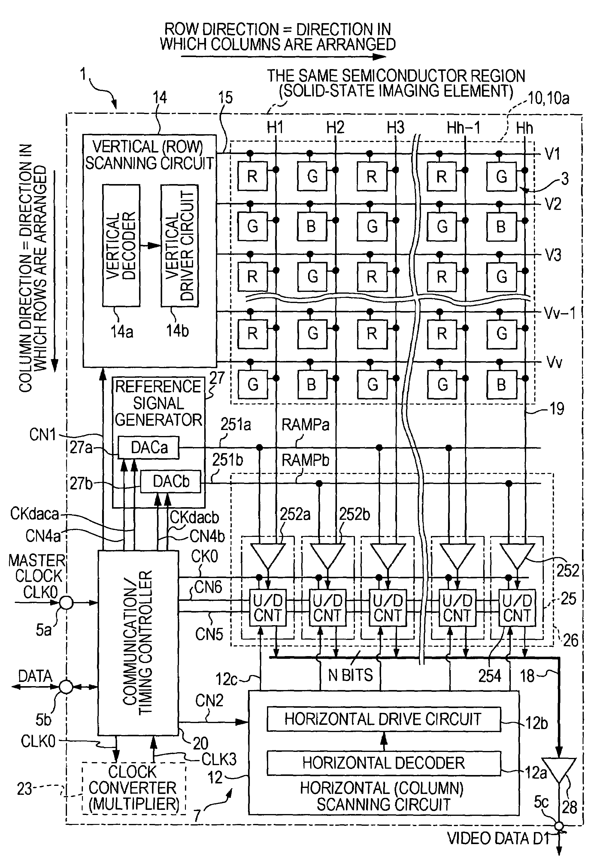
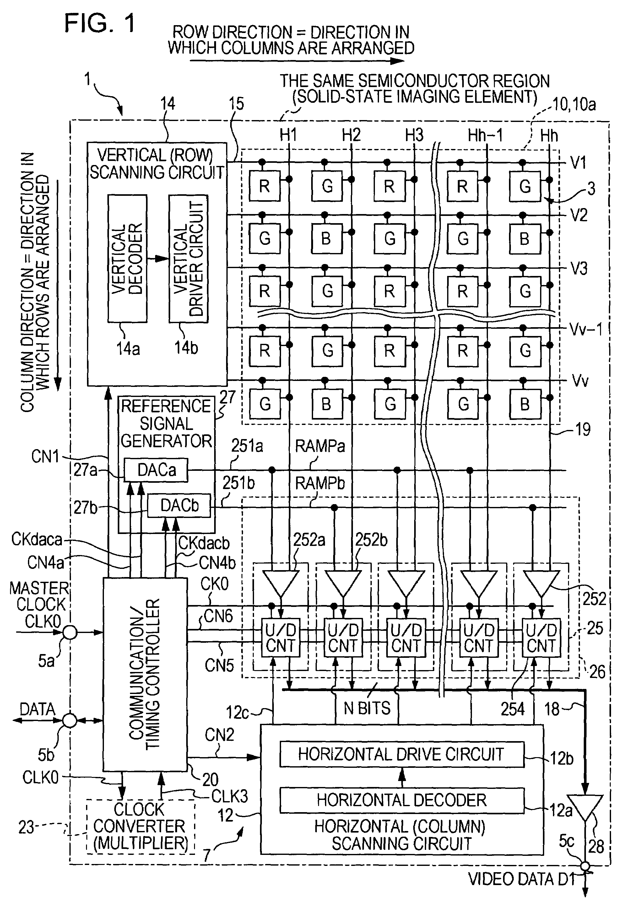
[0037]An embodiment of the present invention is described in detail below with reference to the accompanying drawings in the context of a CMOS-type imaging device, which is an example of an X-Y address solid-state imaging device. A description is given below, assuming that all pixels used in the CMOS-type imaging device are NMOS or PMOS pixels.

[0038]The CMOS-type imaging device is an example only, and the type of device used in the following embodiment is not restricted to a MOS imaging device, and the following embodiment is applicable to all physical-quantity-distribution detecting semiconductor devices including a plurality of unit elements which are disposed in a line or matrix and which are responsive to electromagnetic waves, such as light or radiation, input from an external source.

Configuration of Solid-state Imaging Device

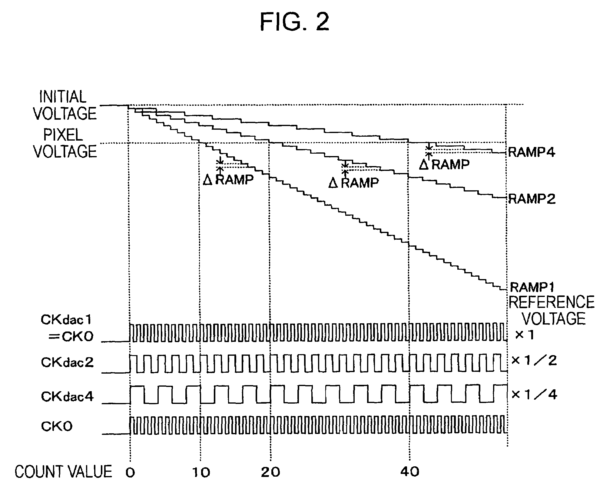
[0039]FIG. 1 is a schematic diagram illustrating a CMOS-type solid-state imaging device (CMOS-type image sensor) 1, which serves as a semiconductor device...


PUM


Abstract

A DA conversion device includes the following elements. A higher-bit current source cell portion includes uniformly weighted higher-bit current source cells to generate an identical constant current. A lower-bit current source cell portion includes a lower-bit current source cells that are weighted to generate 1 / two-to-the-power-of-certain-numbers constant currents. A constant current source selection controller includes a lower-bit controller having a scaler that uses clocks scaled down to 1 / two-to-the-power-of-certain-numbers to select the lower-bit current source cells, and a higher-bit controller having shift registers and using a signal indicating a carry bit or a borrow bit used in the lower-bit controller to sequentially activate shift outputs of the shift registers, and uses the shift outputs to select the higher-bit current source cells. Constant current outputs of the selected current source cells are added and output so that an output current corresponding to the digital input signal is obtained.

Description

CROSS REFERENCES TO RELATED APPLICATIONS[0001]The present invention contains subject matter related to Japanese Patent Application JP 2005-277190 filed in the Japanese Patent Office on Sep. 26, 2005, the entire contents of which are incorporated herein by reference.BACKGROUND OF THE INVENTION[0002]1. Field of the Invention[0003]The present invention relates to a digital-to-analog (DA) converter for converting digital signals into analog signals, an analog-to-digital (AD) converter including this DA converter, and a semiconductor device, such as an imaging device. More particularly, the invention relates to a DA conversion mechanism using a current source cell matrix including an array-structured current source cells.[0004]2. Description of the Related Art[0005]Various DA converters for converting digital signals into analog signals are used in electronic apparatuses.[0006]Physical-quantity-distribution detecting semiconductor devices including a plurality of unit elements (for examp...

Claims


Application Information

Patent Timeline
Patent Type & Authority Patents(United States)
IPC IPC(8): H03M1/66H03M1/56H03M1/68H03M1/74H04N5/335H04N5/357H04N5/374H04N5/378
CPCH03M1/0863H03M1/34H03M1/66H03M1/745H03M1/123H03M1/56H03M1/687H03M1/747H03M1/664
Inventor ASAYAMA, GOFUKUSHIMA, NORIYUKINITTA, YOSHIKAZUMURAMATSU, YOSHINORIAMANO, KIYOTAKA
Owner SONY CORP
Why Eureka
Try Eureka