

Electroluminescent device with anthracene derivative host
an electroluminescent device and host technology, applied in the field of electroluminescent devices of organic origin, can solve the problems of difficult and expensive manufacture of anthracenes in such positions, not providing all desirable, and limiting the performance of anthracenes, etc., to achieve desirable hue, improve operational stability, and high luminance yield
- Summary
- Abstract
- Description
- Claims
- Application Information
AI Technical Summary
Benefits of technology
Problems solved by technology
Method used
Image

Examples
example 1
DEVICE EXAMPLE 1
EL Device Fabrication of Samples 1-6
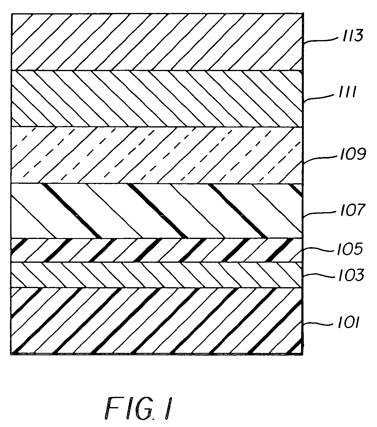
[0180]An EL device (Sample 1) satisfying the requirements of the invention was constructed in the following manner:[0181]1. A glass substrate coated with an 85 nm layer of indium-tin oxide (ITO) as the anode was sequentially ultrasonicated in a commercial detergent, rinsed in deionized water, degreased in toluene vapor and exposed to oxygen plasma for about 1 min.[0182]2. Over the ITO was deposited a 1 nm fluorocarbon (CFx) hole-injecting layer (HIL) by plasma-assisted deposition of CHF3.[0183]3. A hole-transporting layer (HTL) of N,N′-di-1-naphthyl-N,N-diphenyl-4,4′-diaminobiphenyl (NPB) having a thickness of 75 nm was then evaporated from a tantalum boat.[0184]4. A 20 nm light-emitting layer (LEL), including host material Inv-1 and light-emitting material TBP (2,5,8,11-tetra-t-butylperylene, 1.00 vol %), was then deposited onto the hole-transporting layer. These materials were also evaporated from tantalum boats.[0185]5. A 35 nm ...
example 2
DEVICE EXAMPLE 2
EL Device Fabrication of Samples 7-12
[0192]EL devices, Samples 7-11, were fabricated in an identical manner as Sample 1-5, except Inv-1 was replaced with Inv-2. Sample 12 was prepared in the same manner as Sample 6. The devices thus formed were tested for in the same manner as Samples 1-6, except the devices were tested for stability by operating the cells at 20 mA / cm2 for 200 h at 70° C. The testing results are reported in Table 2.
[0193]
TABLE 2Evaluation Results for EL devices 7-12.TBPHostLevelYield200 hSam-Level(vol(cd / Sta-pleHost(nm)%)A)CIExCIEybilityType7Inv-22001.003.350.1640.26486%Invention8Inv-24001.003.270.1740.32184%Invention9Inv-22002.002.880.1650.25789%Invention10Inv-24002.003.300.1750.32987%Invention11Inv-22004.001.710.3110.53880%Invention12TBADN2001.502.860.1440.21783%Com-parison
[0194]It can be seen from Table 2 that the anthracene material of the invention, Inv-2, affords a good luminance yield and operating stability relative to a comparison anthracene...
example 3
DEVICE EXAMPLE 3
EL Device Fabrication of Samples 13-18
[0195]EL devices, Samples 7-11, were fabricated in an identical manner as Sample 1-5, except Inv-1 was replaced with Inv-3. Sample 18 was prepared in the same manner as Sample 6. The devices thus formed were tested for in the same manner as Samples 1-6, except the devices were tested for stability by operating the cells at 20 mA / cm2 for 200 h at 70° C. The testing results are reported in Table 3.
[0196]
TABLE 3Evaluation Results for EL devices 13-18.TBPHostLevelYield200 hSam-Level(vol(cd / Sta-pleHost(nm)%)A)CIExCIEybilityType13Inv-32001.003.520.1700.28588%Invention14Inv-34001.004.260.1740.32887%Invention15Inv-32002.003.440.1700.28591%Invention16Inv-34002.004.140.1750.33589%Invention17Inv-32004.003.150.1770.30989%Invention18TBADN2001.502.870.1420.20575%Com-parison
[0197]It can be seen from Table 3 that the anthracene material of the invention, Inv-3, affords a high luminance yield and very good operating stability relative to a compar...
PUM
| Property | Measurement | Unit |
|---|---|---|
| thick | aaaaa | aaaaa |
| operating voltages | aaaaa | aaaaa |
| wavelength range | aaaaa | aaaaa |
Abstract
Description
Claims
Application Information