

Organic element for electroluminescent devices
a light-emitting diode and electroluminescent technology, applied in the direction of group 3/13 element organic compounds, discharge tube luminescnet screens, natural mineral layered products, etc., can solve the problems of low quantum efficiency of electroluminescence of unsubstituted or alkyl substituted pyrromethene-bf2 complexes, and the inability to obtain luminance efficient green oleds conveniently, etc., to achieve desirable hue and improve luminance efficiency
- Summary
- Abstract
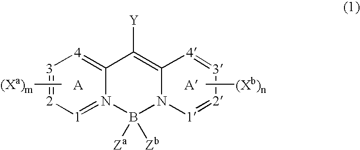
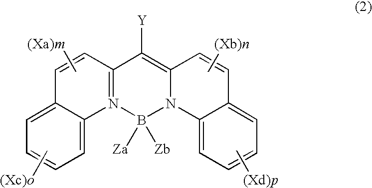
- Description
- Claims
- Application Information
AI Technical Summary
Benefits of technology
Problems solved by technology
Method used
Image

Examples
examples
Maximum Emission and Luminance Efficiency
[0153] Emission spectra were obtained for a series of the above inventive examples and the following comparative examples.
Example# RingsStructureComp-13Comp-24Comp-35
[0154] The emission spectra and quantum yields were obtained at room temperature in ethyl acetate solution at concentrations of 10−5 to 10−6M and expressed as quanta per unit time per unit wavelength interval against wavelength. A fluorescence procedure is well known to those skilled in the art [see, for example, C. A. Parker and W. T. Rees, Analyst, 85, 587 (1960)]. The maximum of emission spectra is defined as the wavelength corresponding to the highest point of such spectrum. The results are shown in the following table.
TABLE 1SOLUTION (ETOAC) DATAExampleTypeE max (soln.)Quantum Yield.Comp-1Comparative492 nm0.15Comp-2Comparative498 nm0.63Comp-3Comparative520 nm0.96Inv-1Inventive490 nm0.72Inv-2Inventive500 nm0.67Inv-3Inventive506 nm0.77Inv-4Inventive476 nm0.86Inv-5Inventi...
example 2
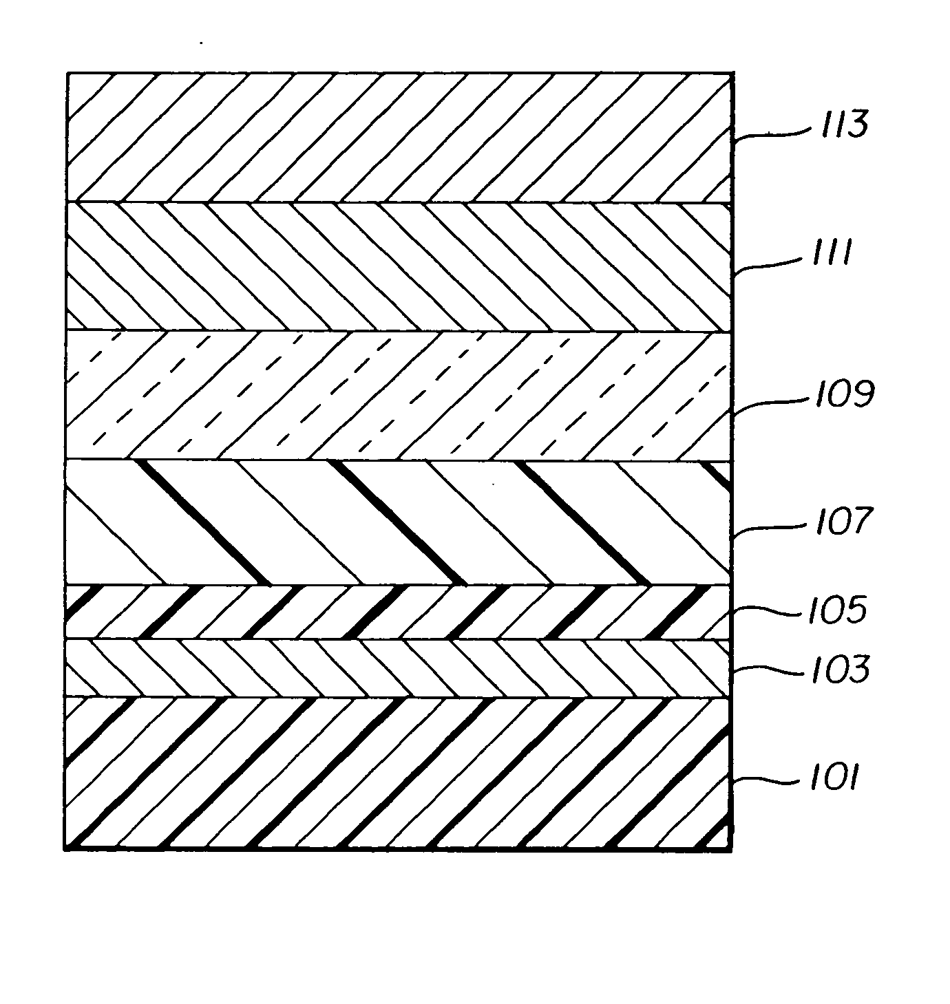
EL Device Fabrication—Inventive Example
[0159] An EL device (Sample 1) satisfying the requirements of the invention was constructed in the following manner: [0160] 1. A glass substrate coated with an 85 nm layer of indium-tin oxide (ITO) as the anode was sequentially ultrasonicated in a commercial detergent, rinsed in deionized water, degreased in toluene vapor and exposed to oxygen plasma for about 1 min. [0161] 2. Over the ITO was deposited a 1 nm fluorocarbon (CFx) hole-injecting layer (HIL) by plasma-assisted deposition of CHF3. [0162] 3. A hole-transporting layer (HTL)of N,N′-di-1-naphthyl-N,N′-diphenyl-4,4′-diaminobiphenyl (NPB) having a thickness of 75 nm was then evaporated from a tantalum boat. [0163] 4. A 25 nm light-emitting layer (LEL) of 2-tert-butyl-9,10-di-(2-naphthyl)anthracene (TBADN) and Inv-1 (0.7% wt %) were then deposited onto the hole-transporting layer. These materials were also evaporated from tantalum boats. [0164] 5. A 35 nm electron-transporting layer (ETL...
example 3
EL Device Fabrication—Inventive Example
[0170] An EL device (Sample 6) satisfying the requirements of the invention was constructed in the following manner: [0171] 1. A glass substrate coated with an 85 nm layer of indium-tin oxide (ITO) as the anode was sequentially ultrasonicated in a commercial detergent, rinsed in deionized water, degreased in toluene vapor and exposed to oxygen plasma for about 1 min. [0172] 2. Over the ITO was deposited a 1 nm fluorocarbon (CFx) HIL by plasma-assisted deposition of CHF3. [0173] 3. A HTL of N,N′-di-1-naphthalenyl-N,N′-diphenyl-4,4′-diaminobiphenyl (NPB) having a thickness of 75 nm was then evaporated from a tantalum boat. [0174] 4. A 37.5 nm LEL of tris(8quinolinolato)aluminum (III) (AlQ3) and Inv-1 (0.7 wt %) were then deposited onto the hole-transporting layer. These materials were also evaporated from tantalum boats. [0175] 5. A 37.5 nm ETL of tris(8quinolinolato)aluminum (III) (AlQ3) was then deposited onto the light-emitting layer. This ma...
PUM
| Property | Measurement | Unit |
|---|---|---|
| wt % | aaaaa | aaaaa |
| wt % | aaaaa | aaaaa |
| wavelength | aaaaa | aaaaa |
Abstract
Description
Claims
Application Information