Power module, and phase leg assembly

a power module and phase leg technology, applied in the direction of printed circuit manufacturing, printed circuit aspects, orthogonal pcbs mounting, etc., can solve the problems of high parasitic inductance of conventional packaging technology, significantly higher electrical stress, and poor current sharing between power devices

Active Publication Date: 2008-02-05
GENERAL ELECTRIC CO
View PDF11 Cites 33 Cited by
  • Summary
  • Abstract
  • Description
  • Claims
  • Application Information

AI Technical Summary

Benefits of technology

[0013]These and other features, aspects, and advantages of the present invention will become better understood when the following detailed description is read with reference to the accompanying drawings in which like characters represent like parts throughout the drawings, wherein:
[0014]FIG. 1 illustrates a single switch power module embodiment of the invention using wire bonds;
[0015]FIG. 2 illustrates another single switch power module embodiment of the invention using a power overlay;
[0016]FIG. 3 is a side view of the single switch power module of FIG. 1 or 2 and schematically depicts an exemplary heat sink for the power module;
[0017]FIG. 4 shows two types of edge card connectors and receptacle configurations;
[0018]FIG. 5 is a cross-sectional view of a phase-leg assembly that includes two exemplary edge card connectors connected to respective receptacles, which are mounted on a back plane;
[0019]FIG. 6 illustrates a phase-leg embodiment of the invention, for clarity the housing is removed, revealing a number of power devices mounted on a substrate;
[0020]FIG. 7 shows the phase-leg of FIG. 6 with the housing in place;
[0021]FIG. 8 is a perspective view of the phase-leg assembly of FIG. 5 with two single switch power modules and a low inductance capacitor mounted on a back-side of a back plane;
[0022]FIG. 9 illustrates a full bridge embodiment of the invention, where several power modules share a heat sink;
[0023]FIG. 10 shows a modular three-phase power converter assembly formed using three of the phase legs shown in FIG. 5;
[0024]FIG. 11 depicts a conventional power module;
[0025]FIG. 12 is an equivalent circuit diagram of an exemplary power module and shows the location of the undesirable parasitic inductances;
[0026]FIG. 13 is an equivalent circuit diagram of an exemplary phase leg assembly and shows the location of the undesirable parasitic inductances;
[0027]FIG. 14 is an equivalent circuit diagram of a three-level phase leg assembly, where the schematic excludes parasitic elements; and
[0028]FIG. 15 is an equivalent circuit diagram for a switched reluctance motor (SRM) embodiment of the invention.

Problems solved by technology

However, inherent to these faster switching transitions are problems associated with the high parasitic inductance of conventional packaging technologies.
In addition to their high parasitic inductance, the non-symmetric layouts result in poor current sharing between power devices.
Accordingly, the use of conventional power modules with the new generation of fast IGBT devices undesirably leads to significantly higher electrical stresses.
However, Mourick et al. fail to address the design of a low parasitic inductance interconnect at the module and converter level.
Other shortcomings of this design include the increased cost due to the addition of conductive webs, as well as the overall complexity of the module assembly.
In addition, the layout is not symmetrical, which can lead to problems with dynamic and static current sharing between parallel power device die.
U.S. Pat. No. 5,574,312, Bayerer et al., entitled “Low-Inductance Power Semiconductor Module,” vaguely describes a low-inductance dual power module built on two-sides of a liquid-cooled heat sink, and there are several aspects of this design that make it impractical.
In addition, soldering of power devices to a double-sided heat sink is less practical and may require the use of multiple solders having different melting temperatures.
This connection would invariably lead to high parasitic inductance, adding to the total phase-leg inductance.

Method used


Image

  • Power module, and phase leg assembly
  • Power module, and phase leg assembly
  • Power module, and phase leg assembly

Examples


Embodiment Construction

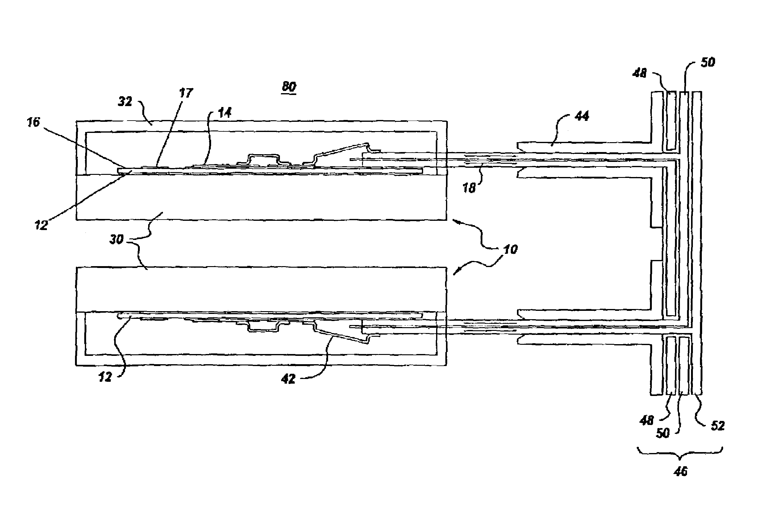
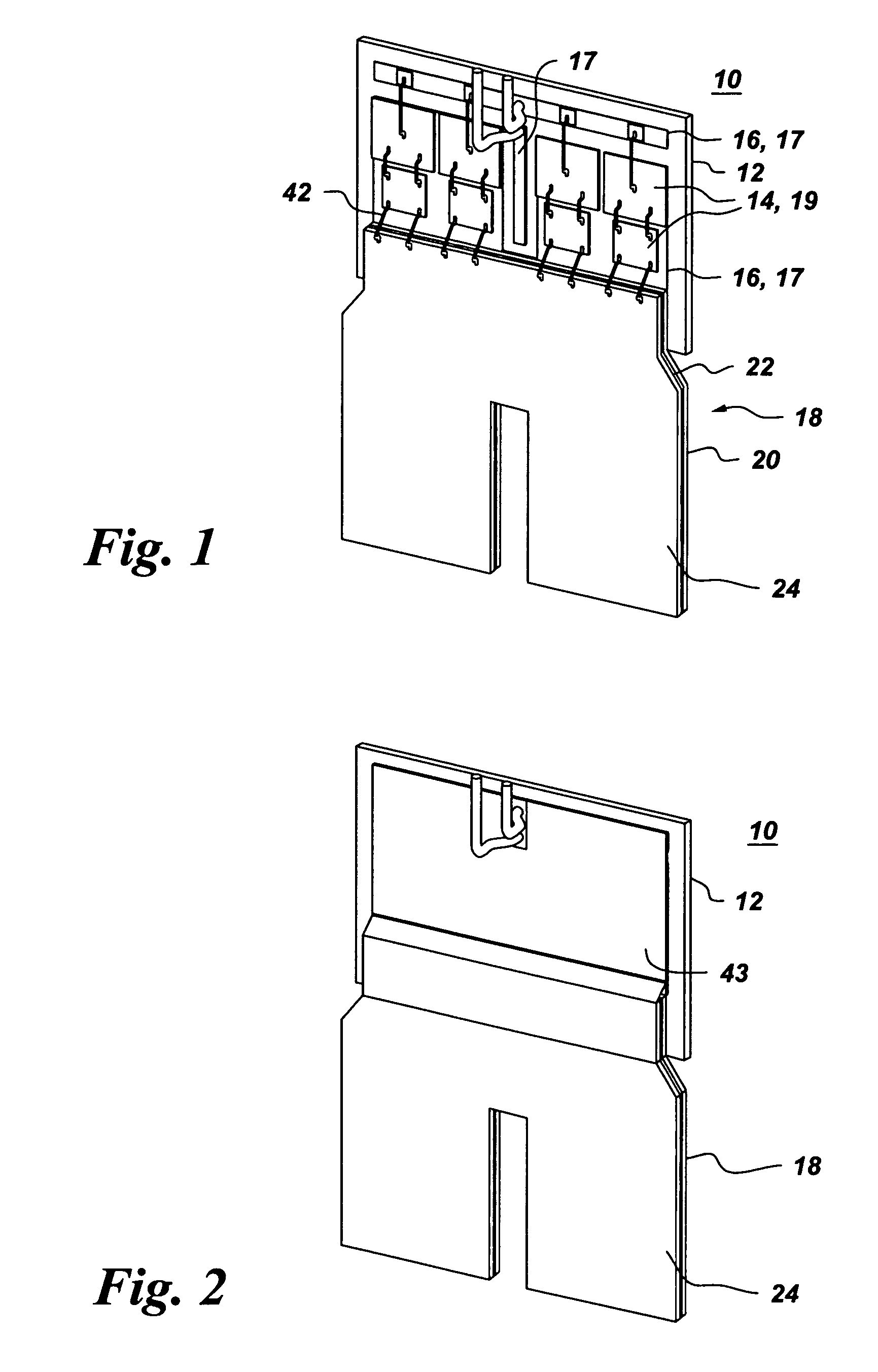
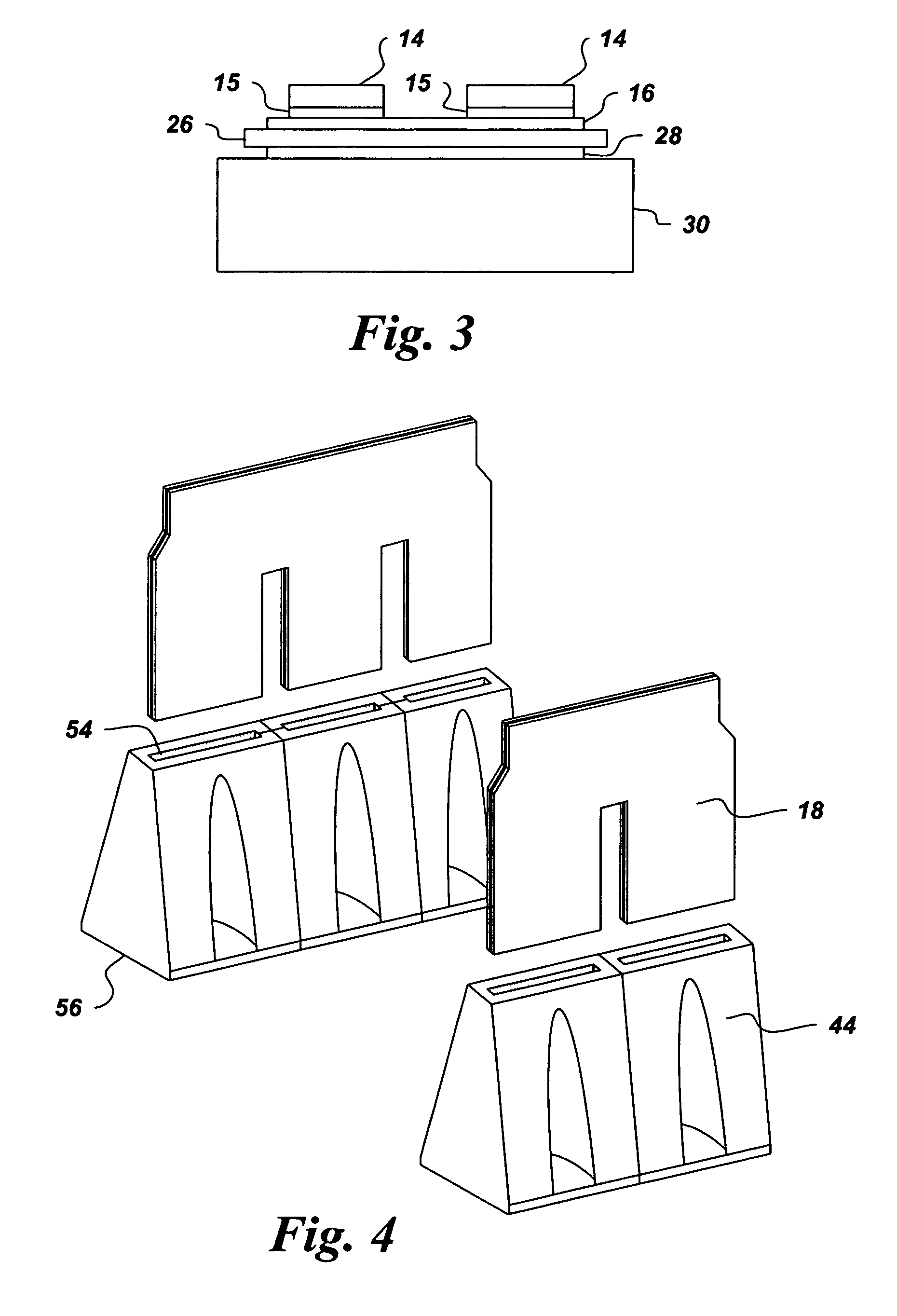
[0029]A single switch power module 10 embodiment of the invention is described with reference to FIGS. 1 and 3. Those skilled in the art will recognize that although power module 10 is described for a single switch configuration, power module 10 is equally applicable to other configurations. As shown, for example, in FIG. 1, power module 10 includes a substrate 12 with an upper layer 16 that includes at least one electrically conductive pattern 17 and is configured for receiving at least one power device 14. An exemplary electrically conductive pattern 17 is illustrated in FIG. 1. As indicated in FIG. 3, substrate 12 further includes an electrical insulator 26 and a thermal coupling layer 28. Electrical insulator 26 is disposed between upper layer 16 and thermal coupling layer 28. Thermal coupling layer 28 is configured for thermal coupling to a heat sink 30. Power module 10 further includes a laminar interconnect 18 that includes a first electrically conductive layer 20, an insulat...


PUM


Abstract

A power module includes a substrate that includes an upper layer, an electrical insulator and a thermal coupling layer. The upper layer includes an electrically conductive pattern and is configured for receiving power devices. The electrical insulator is disposed between the upper layer and the thermal coupling layer. The thermal coupling layer is configured for thermal coupling to a heat sink. The power module further includes at least one laminar interconnect that includes first and second electrically conductive layers and an insulating layer disposed between the first and second electrically conductive layers. The first electrically conductive layer of the laminar interconnect is electrically connected to the upper layer of the substrate. Electrical connections connect a top side of the power devices to the second electrically conductive layer of the laminar interconnect.

Description

CROSS REFERENCE TO RELATED APPLICATIONS[0001]This application is related to commonly assigned, copending U.S. patent application Ser. No. 10 / 998,707 entitled “Heat sink with microchannel cooling for power devices,” Stevanovic et al., filed concurrently herewith, which patent application is incorporated by reference herein in its entirety.BACKGROUND[0002]The invention relates generally to power modules and, more particularly, to low inductance power modules for high power electronic applications.[0003]Modem power semiconductor switches, such as silicon Insulated Gate Bipolar Transistors (IGBTs), are capable of switching at much higher frequencies than earlier designs. Their lower switching losses enable new applications requiring high frequency power conversion. However, inherent to these faster switching transitions are problems associated with the high parasitic inductance of conventional packaging technologies. In particular, the voltage overshoot that occurs when a power device i...

Claims


Application Information

Patent Timeline
Patent Type & Authority Patents(United States)
IPC IPC(8): H01L23/52
CPCH01L24/49H01L25/072H05K1/147H01L24/45H01L25/071H01L2224/45014H01L2224/45015H01L2224/45124H01L2224/48091H01L2224/48137H01L2224/49175H01L2924/01002H01L2924/01004H01L2924/01005H01L2924/01013H01L2924/01014H01L2924/01029H01L2924/01033H01L2924/0105H01L2924/01078H01L2924/01079H01L2924/01082H01L2924/13055H01L2924/13091H01L2924/19041H01L2924/2076H01L2924/30107H01L2924/3011H05K1/0306H05K3/0061H05K3/361H05K2201/044H05K2201/0715H05K2201/10189H05K2201/10287H01L2224/49109H01L2224/49111H01L2924/13063H01L2924/01006H01L2924/01023H01L2924/01068H01L2924/014H01L2224/48472H01L2224/73265H01L2924/13064H01L2924/1306H01L2924/12032H01L2924/1305H01L2924/00014H01L2924/00H01L2224/48139H01L2924/15787H01L2224/49113H01L24/48H01L23/3735H01L2924/206H01L2224/32225H01L2224/48227H01L2924/00012
Inventor STEVANOVIC, LJUBISA DRAGOLJUBDELGADO, ELADIO CLEMENTASCHUTTEN, MICHAEL JOSEPHBEAUPRE, RICHARD ALFREDDE ROOIJ, MICHAEL ANDREW
Owner GENERAL ELECTRIC CO
Why Eureka
Try Eureka