Method for manufacturing multilayer circuit board

a manufacturing method and circuit board technology, applied in the direction of dielectric characteristics, conductive pattern formation, printed element electric connection formation, etc., can solve the problem of relatively complicated manufacturing process and achieve the effect of simplifying the manufacturing process

Inactive Publication Date: 2008-02-12
DENSO CORP
View PDF33 Cites 6 Cited by
  • Summary
  • Abstract
  • Description
  • Claims
  • Application Information

AI Technical Summary

Benefits of technology

[0006]The present invention has been made in view of the above aspects with an object to provide a multilayer circuit board, the manufacturing process of which can be simplified even if the multilayer circuit board has electrodes used for connection with a chip component only on one surface of the board, and to provide a method for manufacturing the multilayer circuit board.

Problems solved by technology

Therefore, the manufacturing process is relatively complicated.

Method used


Image

  • Method for manufacturing multilayer circuit board
  • Method for manufacturing multilayer circuit board
  • Method for manufacturing multilayer circuit board

Examples


first embodiment

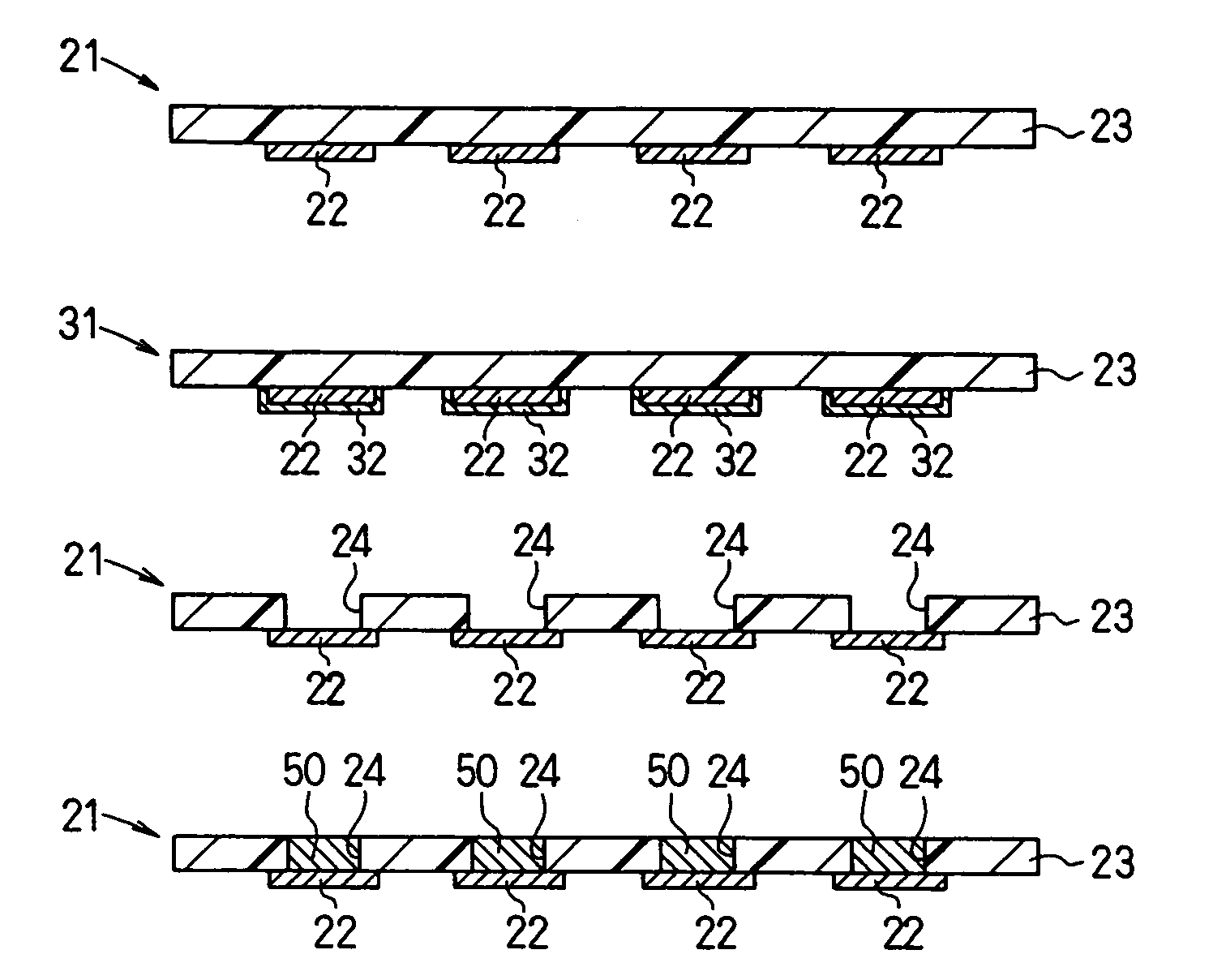
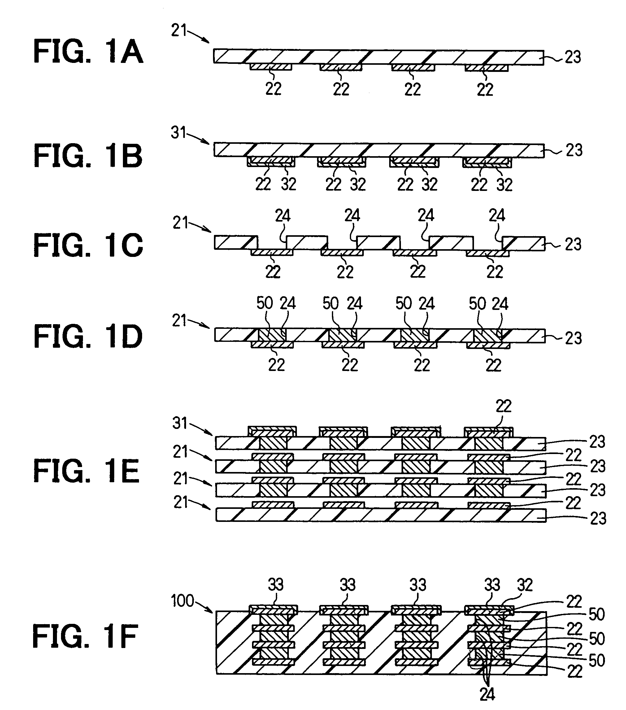
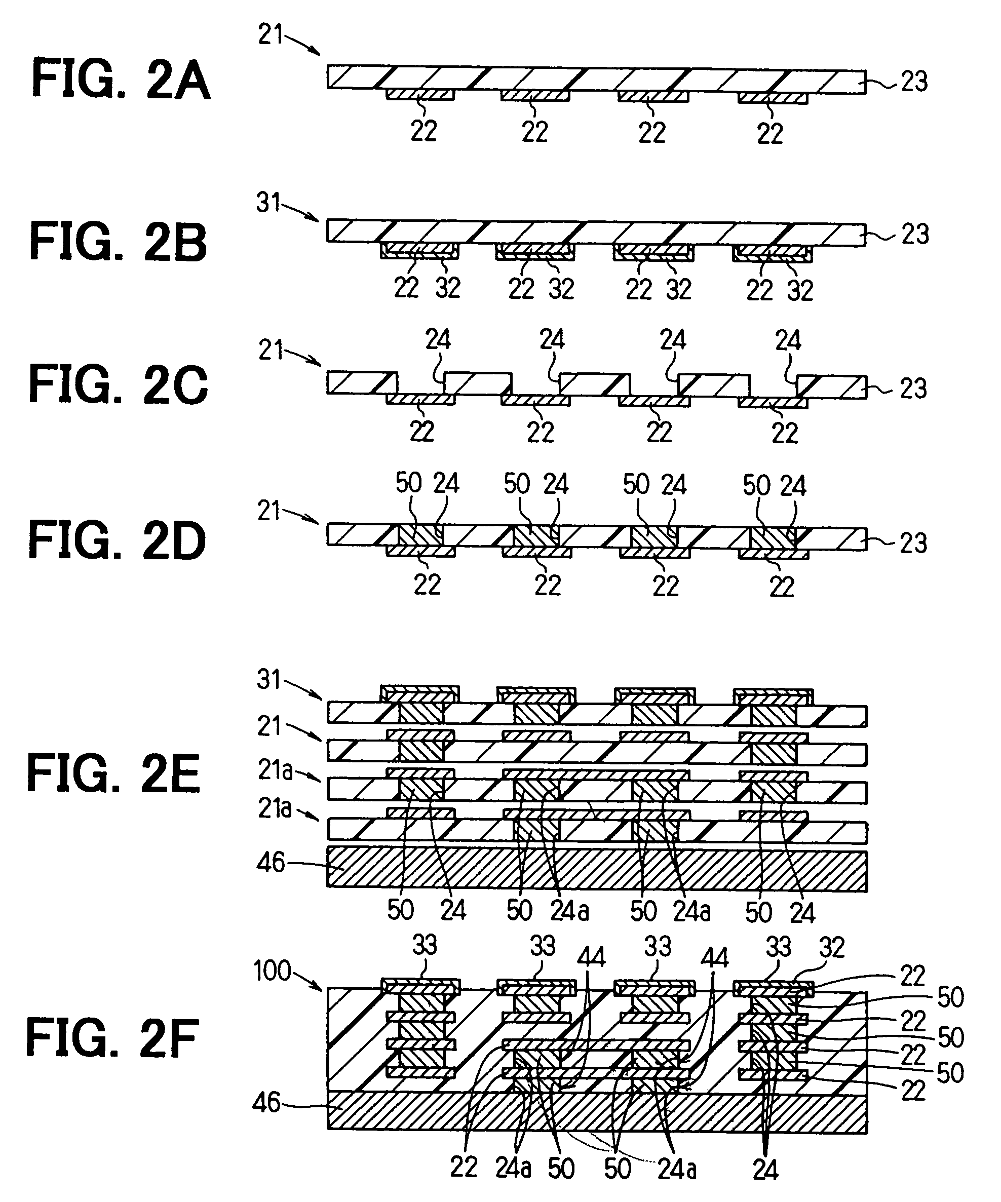
[0012]As shown in FIG. 1A, a single-sided conductor layer film 21 has conductor layers 22, which are shaped by etching a conductive foil (a copper foil with a nominal thickness of 18 micrometers in this embodiment) adhered onto one side of a resin film 23. In FIG. 1A, a thermoplastic film with a thickness of 25-75 micrometers, which is made of a mixture of 65-35 weight % polyetheretherketone resin and 35-65 weight % polyetherimide resin, is used as the resin film 23.

[0013]After the conductor layers 22 are formed as shown in FIG. 1A, to form a single-sided conductor layer film 31 having electrodes 33, which is described later, a single-sided conductor layer film 21 is immersed in plating solutions for so-called nickel-gold plating. Surfaces of the conductor layers 22 are plated with nickel and gold, and as shown in FIG. 1B, processed surface layers 32 are formed on the surfaces of the conductor layers 22. The processed surface layers 32 are formed for the purpose of improving the adh...

second embodiment

[0020]Using steps shown in FIGS. 2A-2D, which are the same steps as those shown in FIGS. 1A-1D in the first embodiment, the conductor layers 22 are formed on the resin films 23, the processed surface layers 32 and the via-holes 24 are formed in the resin films 23, and the conductive paste 50 is packed in the via-holes 24. A plurality of single-sided conductor layer films 21a are formed using the same steps as for the single-sided conductor layer films 21. Each single-sided conductor layer film 21a includes a plurality of thermal vias 44, which are made of via-holes 24a and the conductive paste 50, which is packed in the via-holes 24a.

[0021]After the conductive paste 50 is packed in the via-holes 24, 24a of the single-sided conductor layer films 21, 21a, 31, as shown in FIG. 2E, a plurality of single-sided conductor layer films 21, 21a (three films in this embodiment) are stacked such that the surfaces having the conductor layers 22 face upward. On top of the stacked single-sided co...


PUM

PropertyMeasurementUnit
elastic modulusaaaaaaaaaa
thicknessaaaaaaaaaa
thicknessaaaaaaaaaa

Abstract

A multilayer circuit board that has electrodes only on one surface is manufactured as follows. A plurality of conductor layers are formed on a resin film made of thermoplastic resin to form a single-sided conductor layer film. Then, a plurality of via-holes 24, which are bottomed by the conductor layers, are formed in the resin film. Then interlayer connecting material is packed in the via-holes 24 to form a single-sided conductor layer film having the interlayer connecting material. A plurality of single-sided conductor layer films are formed and stacked such that surfaces having the conductor layers face in the same direction. Then, the single-sided conductor layer films are pressed and heated to complete the multilayer circuit board. The multilayer circuit board is formed by using only the single-sided conductor layer films and pressing once, so the manufacturing process is simplified.

Description

CROSS REFERENCE TO RELATED APPLICATION[0001]This application is a divisional application of U.S. patent application Ser. No. 10 / 179,203, which was filed on Jun. 26, 2002, now U.S. Pat. No. 6,768,061.BACKGROUND OF THE INVENTION[0002]The present invention relates to a multilayer circuit board and a method for manufacturing the multilayer circuit board, especially relates to a multilayer circuit board that has electrodes, which are used for the connection with a chip component, only on one surface of the board and to a method for manufacturing the multilayer circuit board.[0003]A conventionally known multilayer circuit board of the same type is manufactured using a plurality of so-called double-sided boards as follows. Each double-sided board includes a thermosetting resin film and a plurality of conductor layers, which are located on two surfaces of the thermosetting resin film. The conductor layers on one surface are electrically connected to the conductor layers on the other surface...

Claims


Application Information

Patent Timeline
Patent Type & Authority Patents(United States)
IPC IPC(8): H05K3/10H05K1/11H05K1/02H05K1/05H05K3/24H05K3/40H05K3/46
CPCH05K3/4617H05K3/4632H01L2224/1147H05K1/0206H05K1/056H05K3/244H05K3/4069Y10T29/49155H05K2201/0129H05K2201/0394H05K2203/072Y10T29/49128Y10T29/49163Y10T29/4913H05K3/46
Inventor KONDO, KOJI
Owner DENSO CORP
Why Eureka
Try Eureka