Check patentability & draft patents in minutes with Patsnap Eureka AI!

Method for forming a plated microvia interconnect

a technology of micro-via and interconnecting parts, applied in the field of interconnecting parts, can solve the problems of increasing difficulty in providing landing areas with small and reliable receptor pads, increasing difficulty in achieving current design techniques, and achieving the effect of high-density surface mounting technology

Inactive Publication Date: 2008-02-12
INVENSAS CORP
View PDF45 Cites 2 Cited by
  • Summary
  • Abstract
  • Description
  • Claims
  • Application Information

AI Technical Summary

Benefits of technology

[0013]It is therefore an advantage of the present invention to provide a microvia structure that can be used as a receptor pad and directly receive a solder deposit.
[0014]It is therefore a further advantage of the present invention to provide higher density surface mounting technology by eliminating the need for dog bones and the like.
[0015]It is therefore a further advantage of the present invention to provide a microvia that allows solder to reliably wet thereon.

Problems solved by technology

Forming electrical connections between components remains an ongoing challenge in the electronics industry.
While soldering techniques are widely available to connect components, the ability to provide landing areas with small and reliable receptor pads becomes increasingly difficult.
This is becoming more difficult to achieve with present design techniques.
If such a surface is not provided, solder often fails to properly wet the pads and becomes inadvertently removed from the pad during subsequent reflow and wash processes.
Unfortunately, these structures take up a lot of surface area.

Method used


Image

  • Method for forming a plated microvia interconnect
  • Method for forming a plated microvia interconnect
  • Method for forming a plated microvia interconnect

Examples


Embodiment Construction

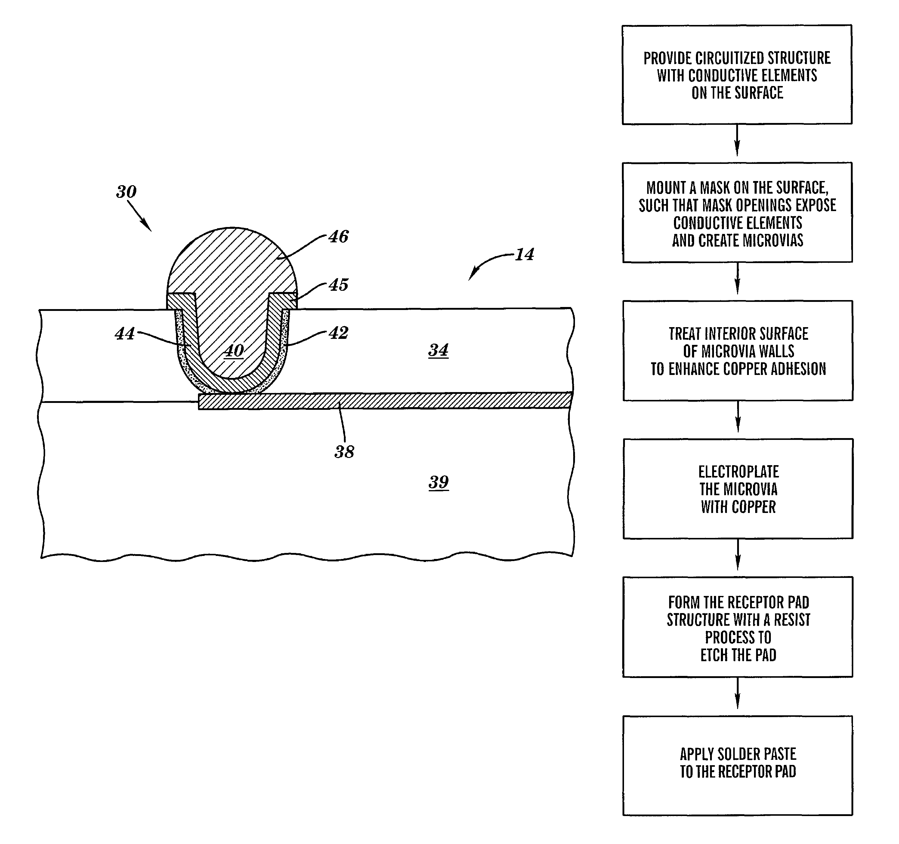
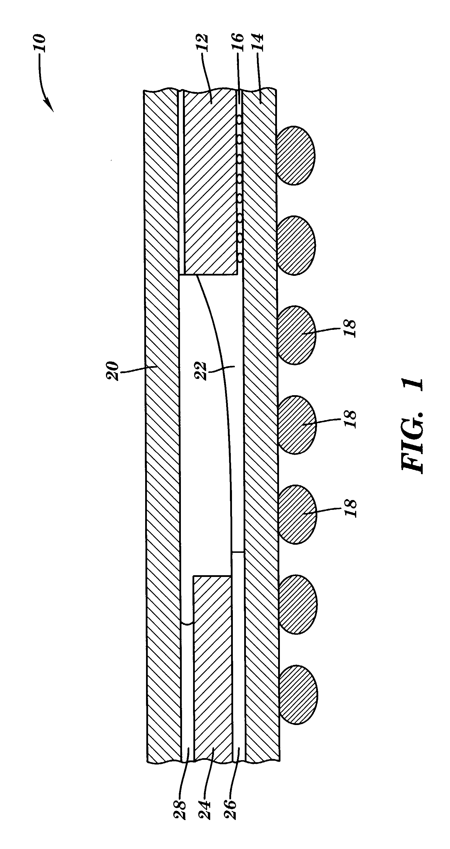
[0021]Referring to figures, FIG. 1 depicts a cross-section of a integrated circuit chip package 10. The integrated circuit chip package 10 includes a chip 12, a laminate 14, connections 16 that interconnect the laminate 14 with the chip 12, a cover plate 20, a stiffener 24, adhesives 26 and 28, an encapsulation material 22, and a ball grid array (BGA) structure 18. While this preferred embodiment deals generally with the electrical interconnect between laminate 14 and chip 12 within a chip package, it is understood that the structure and methods described herein could be used on any planarized surface that provides component interconnections. Moreover, the figures are provided primarily for explanation purposes, and are not necessarily drawn to scale.

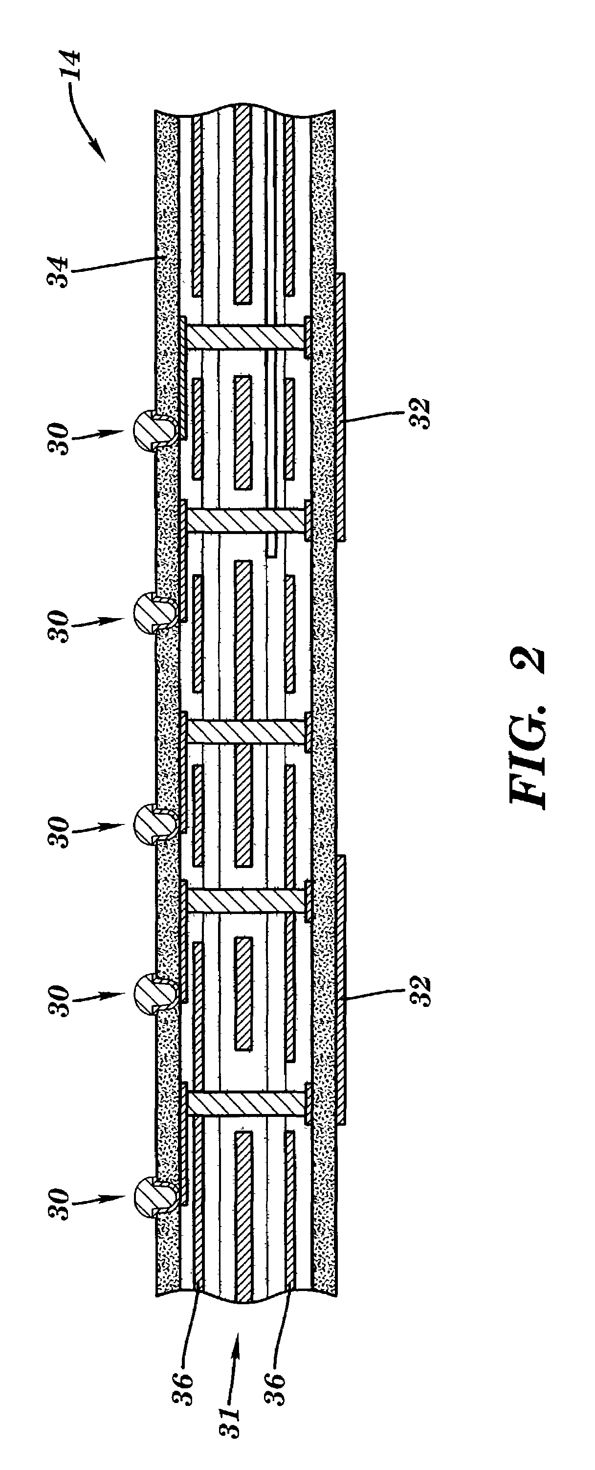
[0022]Referring now to FIG. 2, the laminate 14 is depicted in detail, and includes receptor pads 30 on a top surface, BGA pads 32 on a bottom surface, a circuitized substrate 31, and an external dielectric layer (EDL) 34 mounted on the ...


PUM

PropertyMeasurementUnit
thicknessaaaaaaaaaa
thicknessaaaaaaaaaa
diameteraaaaaaaaaa

Abstract

A method for forming a plated microvia interconnect. An external dielectric layer (EDL) is mounted on a surface of the substrate and is in direct mechanical contact with a conductive element included in the surface. An opening formed in the EDL exposes the conductive element and creates a microvia in the EDL. A sidewall and bottom wall surface of the microvia is treated to promote copper adhesion to the sidewall and bottom wall surfaces. The sidewall and bottom wall surfaces are plated to form a layer of copper thereon. The layer of copper is in direct mechanical and electrical contact with the conductive element. A wet solder paste deposited on the layer of copper overfills a remaining portion of the microvia. The solder paste is reflowed to form a solder bump in and over the remaining portion of the microvia to form the plated microvia interconnect.

Description

[0001]This application is a divisional of Ser. No. 09 / 340,758, filed on Jun. 28, 1999 now U.S. Pat. No. 6,492,600.BACKGROUND OF THE INVENTION[0002]1. Technical Field[0003]The present invention relates to interconnect structures, and more specifically relates to a receptor pad for use in a chip carrier package.[0004]2. Prior Art[0005]Forming electrical connections between components remains an ongoing challenge in the electronics industry. As sizes decrease, more precision and smaller interconnections are required when attaching components to circuit boards, planar surfaces, substrates, and the like (collectively referred to herein as “landing areas”). While soldering techniques are widely available to connect components, the ability to provide landing areas with small and reliable receptor pads becomes increasingly difficult.[0006]One particular application that utilizes high density interconnections involves integrated circuit (IC) chip packaging. An IC chip package comprises a rel...

Claims


Application Information

Patent Timeline
Patent Type & Authority Patents(United States)
IPC IPC(8): H01K3/10H01L21/48H01L23/498H05K1/11H05K3/28H05K3/34H05K3/42H05K3/46
CPCH01L21/4853H01L21/486H01L23/49816H05K1/112H05K3/3484H01L21/4857Y10T29/49155H01L23/49822H01L23/49827H05K3/28H05K3/3457H05K3/429H05K3/4602H05K2201/09436H05K2201/09509H05K2201/09863H05K2203/043H01L2224/16225H01L2224/32225H01L2224/73204H01L2224/73253H01L2924/15311Y10T29/49165H01L2924/00H05K3/3485
Inventor JIMAREZ, MIGUEL A.KEESLER, ROSS W.MARKOVICH, VOYA R.RAI, RAJINDER S.TYTRAN-PALOMAKI, CHERYL L.
Owner INVENSAS CORP
Features
  • R&D
  • Intellectual Property
  • Life Sciences
  • Materials
  • Tech Scout
  • Unparalleled Data Quality
  • Higher Quality Content
  • 60% Fewer Hallucinations
Learn More