Method for producing silicon wafer

a technology of silicon wafers and silicon wafer substrates, applied in the direction of polycrystalline material growth, crystal growth process, protective fluid, etc., can solve the problems of increased production yield, increased production cost, and increased production cost. , to achieve the effect of high pull rate, good yield and increased production yield

Active Publication Date: 2008-02-12
SUMCO TECHXIV
View PDF12 Cites 6 Cited by
  • Summary
  • Abstract
  • Description
  • Claims
  • Application Information

AI Technical Summary

Benefits of technology

[0024]With the foregoing in view, a first object of the present invention is to determine the lower limit LN1 of epitaxial defect-free region α2 and thereby make it possible to manufacture in a good yield high-quality epitaxial silicon wafers which are free of epitaxial defects.
[0061]By controlling the oxygen concentration within the silicon crystal to a low concentration of 12.5×10¹⁷ atoms / cm3 or less in accordance with the tenth aspect of the invention, even if the crystal production conditions region extends into the epitaxial defect region β1, no OSF nuclei in the silicon wafer substrate grow into OSFs and appear as epitaxial defects in the epitaxial growth layer. The conditions for setting the boron concentration and growth condition V / G can thus be relaxed, enabling the production yield to be increased even further.

Problems solved by technology

However, in the course of silicon crystal growth, crystal defects known as “grown-in defects” arise.
With the progress in recent years toward higher density and smaller geometries in semiconductor circuits, the presence of such grown-in defects near the surface layer of the silicon wafer where devices are fabricated can no longer be tolerated.
However, in recent years, as the systems used to inspect defects have become increasingly sensitive and the criteria for evaluating defects have become more exacting, it has been found that defects within the silicon wafer substrate propagate to the epitaxial growth layer, where they appear as defects in the epitaxial growth layer (referred to herein as “epitaxial defects”).
Grown-in defects in a silicon wafer substrate include defects which readily propagate to the epitaxial growth layer and defects which do not readily propagate.
OSFs and dislocation loop clusters in particular are very likely to propagate to the epitaxial growth layer and become epitaxial defects, and so must be excluded from the silicon wafer substrate.

Method used


Image

  • Method for producing silicon wafer
  • Method for producing silicon wafer
  • Method for producing silicon wafer

Examples


Embodiment Construction

[0068]Embodiments of the silicon wafer production methods of the invention are described below in conjunction with the attached diagrams.

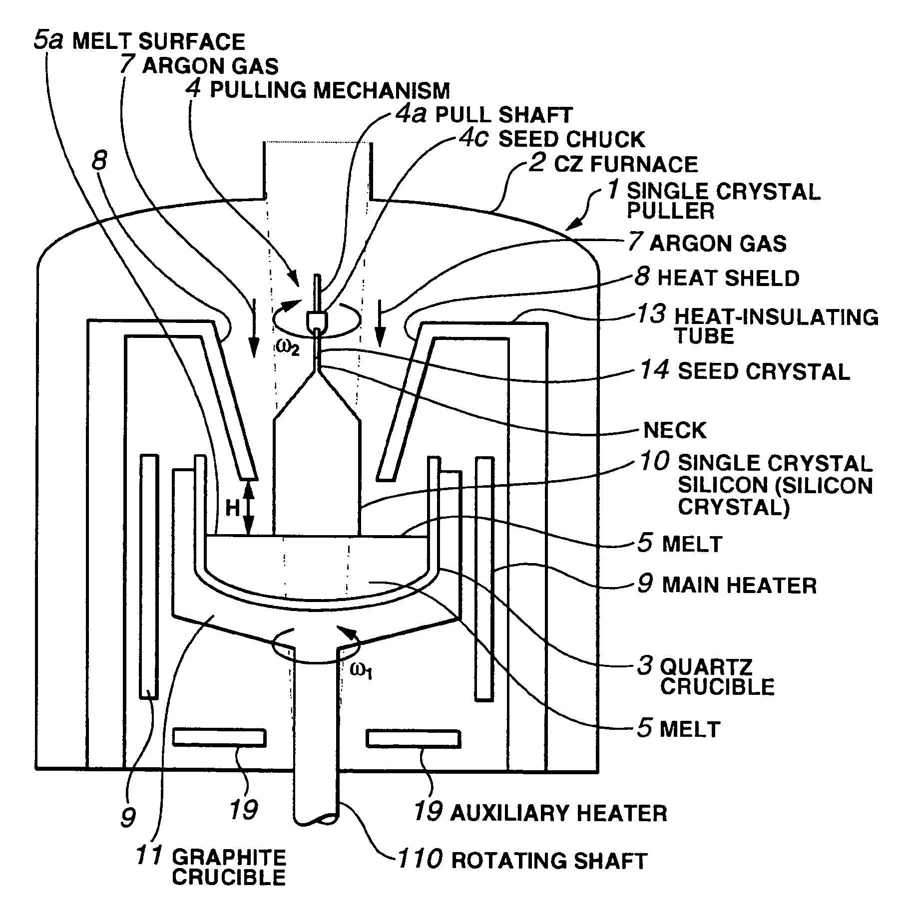
[0069]FIG. 4 is a side view showing the construction of a silicon crystal production apparatus such as may be used in the embodiments of the invention.

[0070]Referring to FIG. 4, a single crystal puller 1 according to this embodiment has a CZ furnace (chamber) 2 as the single crystal pulling enclosure.

[0071]Inside the CZ furnace 2, there is provided a quartz crucible 3 which melts the polysilicon starting material and holds it as a melt 5. The quartz crucible 3 is covered on the outside with a graphite crucible 11. A main heater 9 which heats and melts the polysilicon starting material inside the quartz crucible 3 is provided outside of and lateral to the quartz crucible 3. Below the quartz crucible 3, there is provided an auxiliary heater (bottom heater) 19 which additionally heats the base of the quartz crucible 3 to prevent solidification of the ...


PUM

PropertyMeasurementUnit
thicknessaaaaaaaaaa
thicknessaaaaaaaaaa
temperatureaaaaaaaaaa

Abstract

The present invention is to produce a silicon crystal wherein the boron concentration in the silicon crystal and the growth condition V / G are controlled so that the boron concentration in the silicon crystal is no less than 1×10¹⁸ atoms / cm3 and the growth condition V / G falls within the epitaxial defect-free region α2 whose lower limit line LN1 is the line indicating that the growth rate V gradually drops as the boron concentration increases. A silicon wafer is also produced wherein the boron concentration in the silicon crystal and the growth condition V / G are controlled so as to include at least the epitaxial defect region β1, and both the heat treatment condition and the oxygen concentration of the silicon crystal are controlled so that no OSF nuclei grow to OSFs.

Description

TECHNICAL FIELD[0001]The present invention relates to a method for producing silicon wafers, and more particularly to a method which, during the production of a silicon wafer on which an epitaxial growth layer is formed, can make the epitaxial layer free of defects.BACKGROUND ART[0002]Silicon crystals are produced by being pulled and grown using the Czochralski (CZ) method. The grown silicon crystal ingot is then sliced into silicon wafers. Semiconductor devices are fabricated by operations in which device layers are formed on the surface of the silicon wafer.[0003]However, in the course of silicon crystal growth, crystal defects known as “grown-in defects” arise.[0004]With the progress in recent years toward higher density and smaller geometries in semiconductor circuits, the presence of such grown-in defects near the surface layer of the silicon wafer where devices are fabricated can no longer be tolerated. This situation has led to explorations on the possibility of manufacturing...

Claims


Application Information

Patent Timeline
Patent Type & Authority Patents(United States)
IPC IPC(8): C30B15/00C30B21/06C30B23/00C30B27/02C30B30/04C30B29/06C30B15/04C30B15/22H01L21/322H01L21/324
CPCC30B29/06C30B15/203
Inventor MAEDA, SUSUMUINAGAKI, HIROSHIKAWASHIMA, SHIGEKIKUROSAKA, SHOEINAKAMURA, KOZO
Owner SUMCO TECHXIV
Why Eureka
Try Eureka