

Device for contacting patterned electrodes on porous substrates
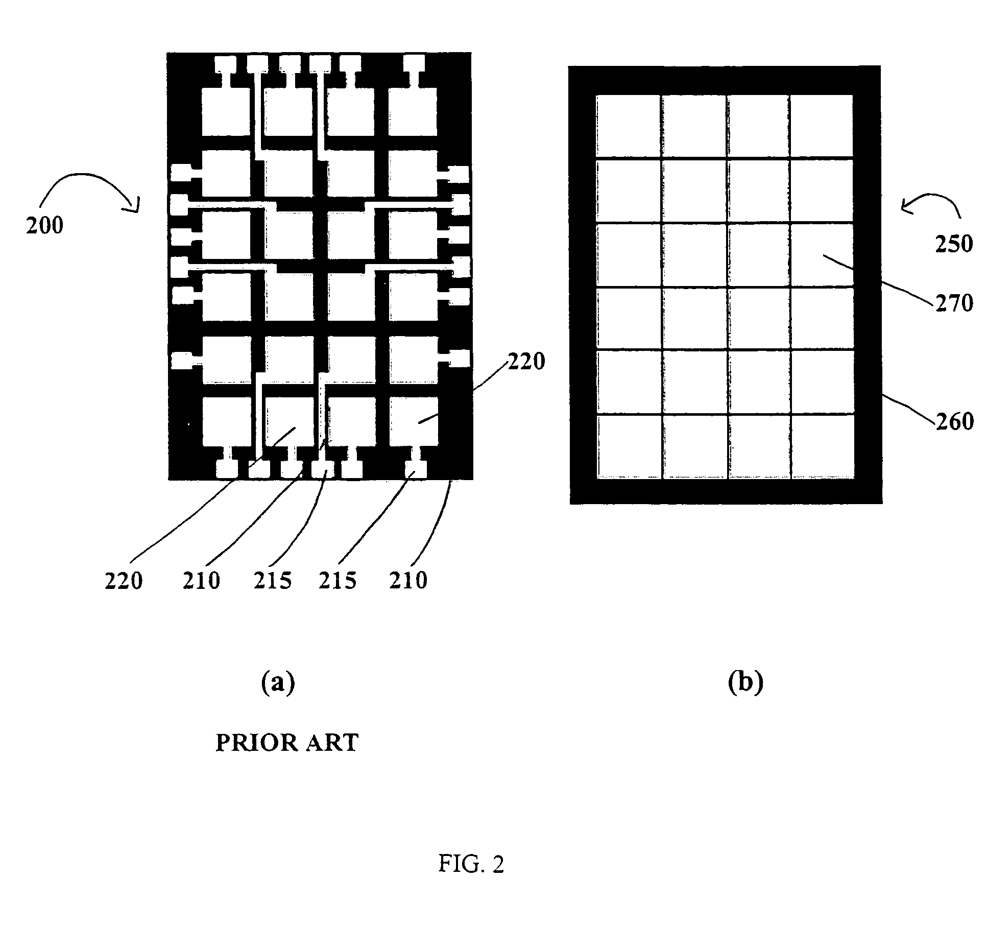
a technology of porous substrates and electrodes, applied in variable capacitors, generators/motors, instruments, etc., can solve the problems of performance limitations, affecting the appearance of the device for display applications, and reducing the available area of active devices
- Summary
- Abstract
- Description
- Claims
- Application Information
AI Technical Summary
Benefits of technology
Problems solved by technology
Method used
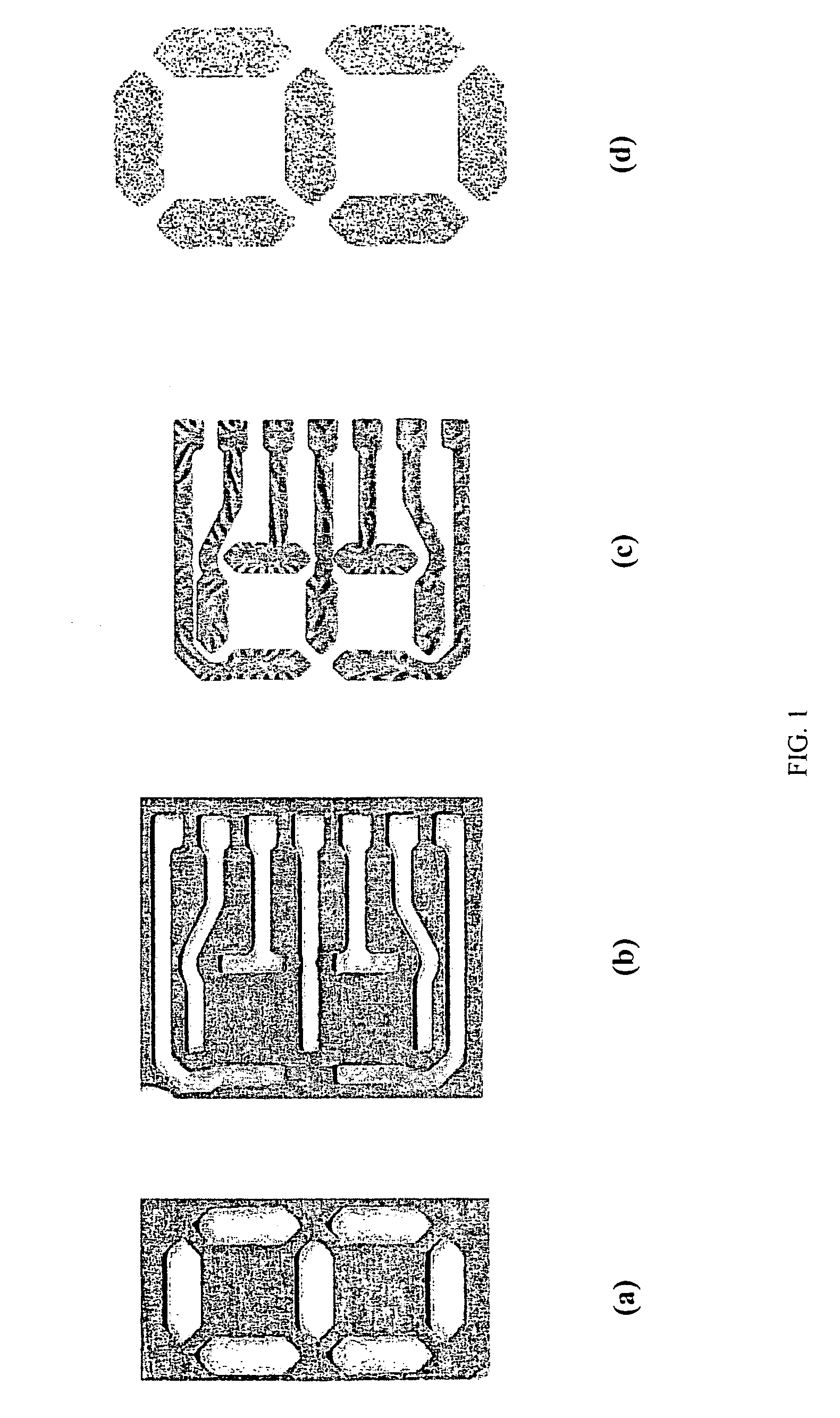
Image

Examples
examples
[0065]The present invention is further illustrated by the following specific simulation Examples, which should not be construed as limiting the scope or content of the invention in any way.
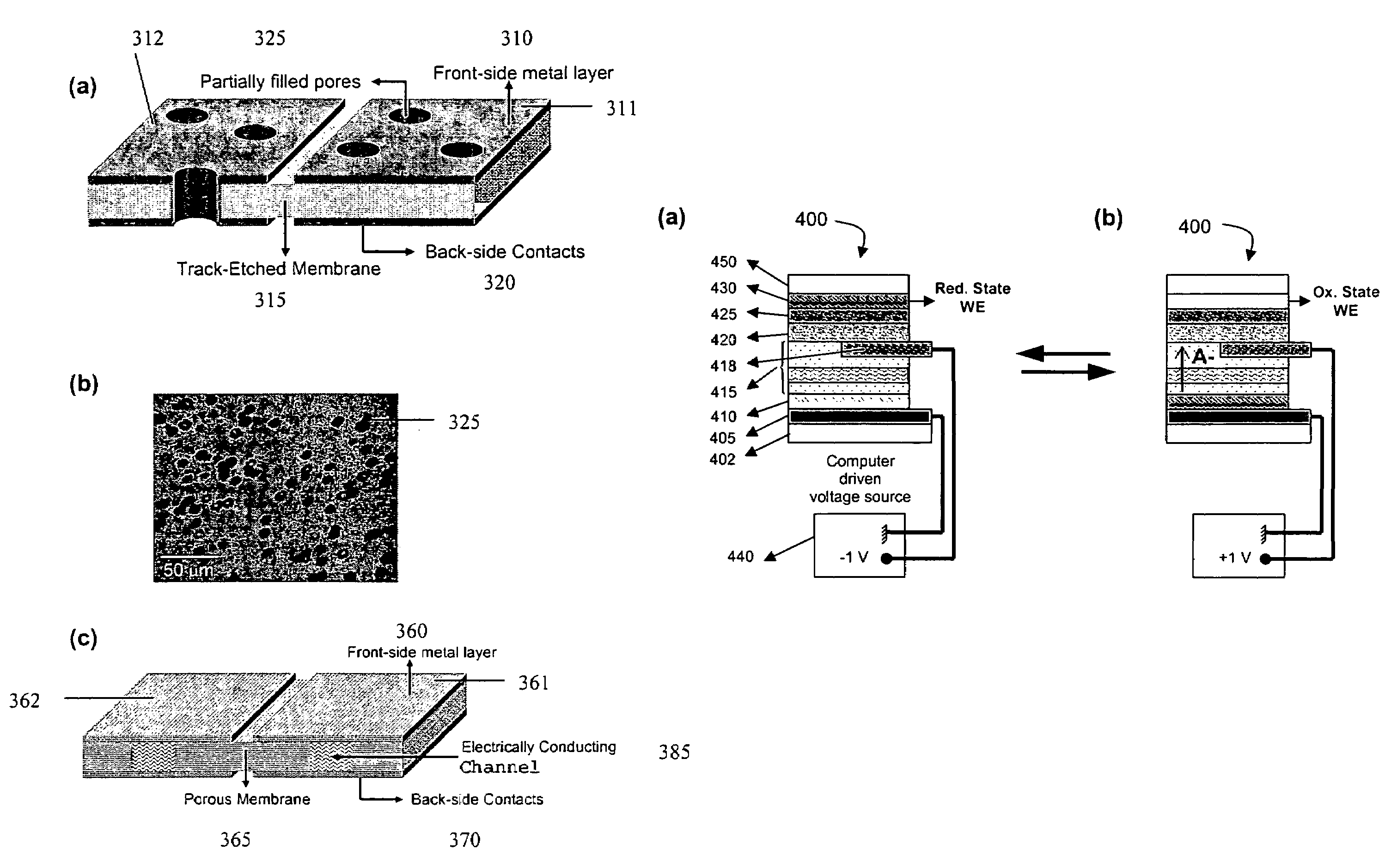
[0066]The Examples below relate to an exemplary application of the invention to ECDs. The ECDs comprise electrochromic polymer(s) which cover a reflective gold surface mounted onto a uniformly porous substrate using patterning techniques. Following a layer-by-layer configuration, the electro-active platforms were paired to a polymeric counter-electrode in order to assemble reflective ECDs. Alkylenedioxythiophenes-based polymers are described on porous architectures with back side contact according to the invention to build fast switchable and highly stable ECDs which require a very low energy to maintain a reflective or absorptive property.
[0067]Propylene carbonate (PC) and acetonitrile (ACN) were purchased from Aldrich, distilled and dried before use. LiClO4 (99%, purity) was purchased from Fluka...
PUM
| Property | Measurement | Unit |
|---|---|---|
| thickness | aaaaa | aaaaa |
| band gap | aaaaa | aaaaa |
| band gap | aaaaa | aaaaa |
Abstract
Description
Claims
Application Information