Silicon single crystal, and process for producing it

a single crystal, silicon technology, applied in the direction of crystal growth process polycrystalline material growth, etc., can solve the problem of difficult adjustment of heat-transferring melt flow, difficulty in deliberately setting radial crystal properties within the narrowest possible range, and inability to complete the theoretical calculation in advance. problem

Inactive Publication Date: 2008-02-26
SILTRONIC AG
View PDF19 Cites 8 Cited by
  • Summary
  • Abstract
  • Description
  • Claims
  • Application Information

AI Technical Summary

Benefits of technology

[0019]It is an object of the present invention to provide an improved process allowing the concentration of internal defects and of foreign substances such as oxygen and dopant in the radial direction to be set in a targeted fashion within a narrow range.
[0022]The inventors of the process described below have discovered that a targeted disruption to the rotational symmetry of the temperature field in the melt, in particular in the region of the solidification interface, has the effect of making the axial temperature gradient G(r) and the concentration of oxygen and dopants more uniform over the crystal diameter. This effect also manifests itself, for example, in the fact that the curvature of the solidification interface is significantly reduced compared to when a rotationally symmetrical temperature field is used.
[0026]Metallic materials, such as for example copper plates with a thickness of one or a few centimeters, which are arranged inside the magnet coils, can be used as magnetic shields. The depth of penetration of dynamic magnetic fields is dependent on the frequency used. Therefore, frequencies of 10 Hz to approximately 1000 Hz are used. When using traveling magnetic fields with partial shielding in the form of rectangular copper plates, a frequency in the region of 30 Hz is particularly suitable. The strength of the magnetic field also determines its effect. Current intensities of preferably up to 500 A in the case of up to 50 coil turns are used to generate alternating fields. High crucible rotational speeds, in particular rotations of 3 rpm and above, reduce the influence of the magnetic field, i.e. the desired non-rotationally symmetrical effect on the melt flows then decreases significantly. The quantity of melt which is in each case present in the crucible should also be taken into account, since different melt flow patterns can form as a function of this quantity. The required conditions, i.e. the ratio of magnetic field, shielding and pulling process parameters, such as for example the crucible rotation, are in each case determined in more detail by experiments and by simulation calculations for estimation purposes.

Problems solved by technology

In particular, there are considerable difficulties with deliberately setting the radial crystal properties within the narrowest possible range.
Adjusting the heat-transferring melt flows often proves difficult, since complete theoretical calculation in advance is very complicated.
They generally have diameters of approximately 100 nm and may cause problems during component fabrication.
In general, even epitaxial layers can no longer cover these defects without any flaws.
Consequently, these defects may adversely affect the yield of components.
However, this is not easy to achieve, in particular if single crystals with a relatively large diameter are being pulled, since the value of G is then significantly dependent on the radius.
However, homogenizing the temperature gradient using these methods becomes more and more difficult with large single crystals.

Method used


Image

  • Silicon single crystal, and process for producing it
  • Silicon single crystal, and process for producing it
  • Silicon single crystal, and process for producing it

Examples


examples

[0043]The text which follows uses examples to explain the effect of arrangements according to the invention by comparison with conventional arrangements in more detail.

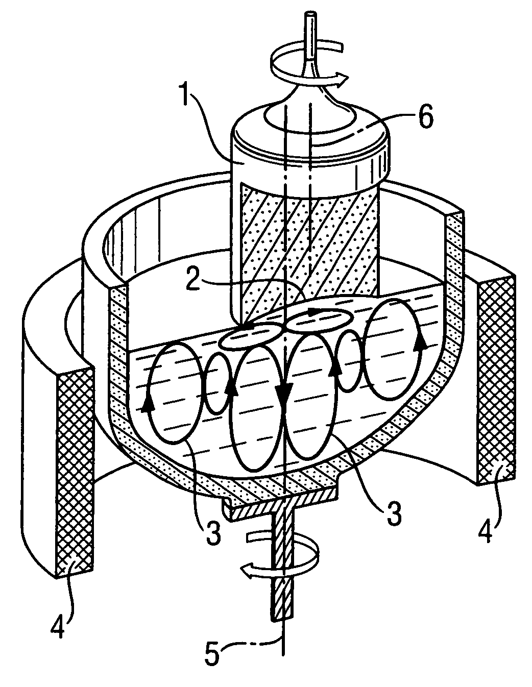
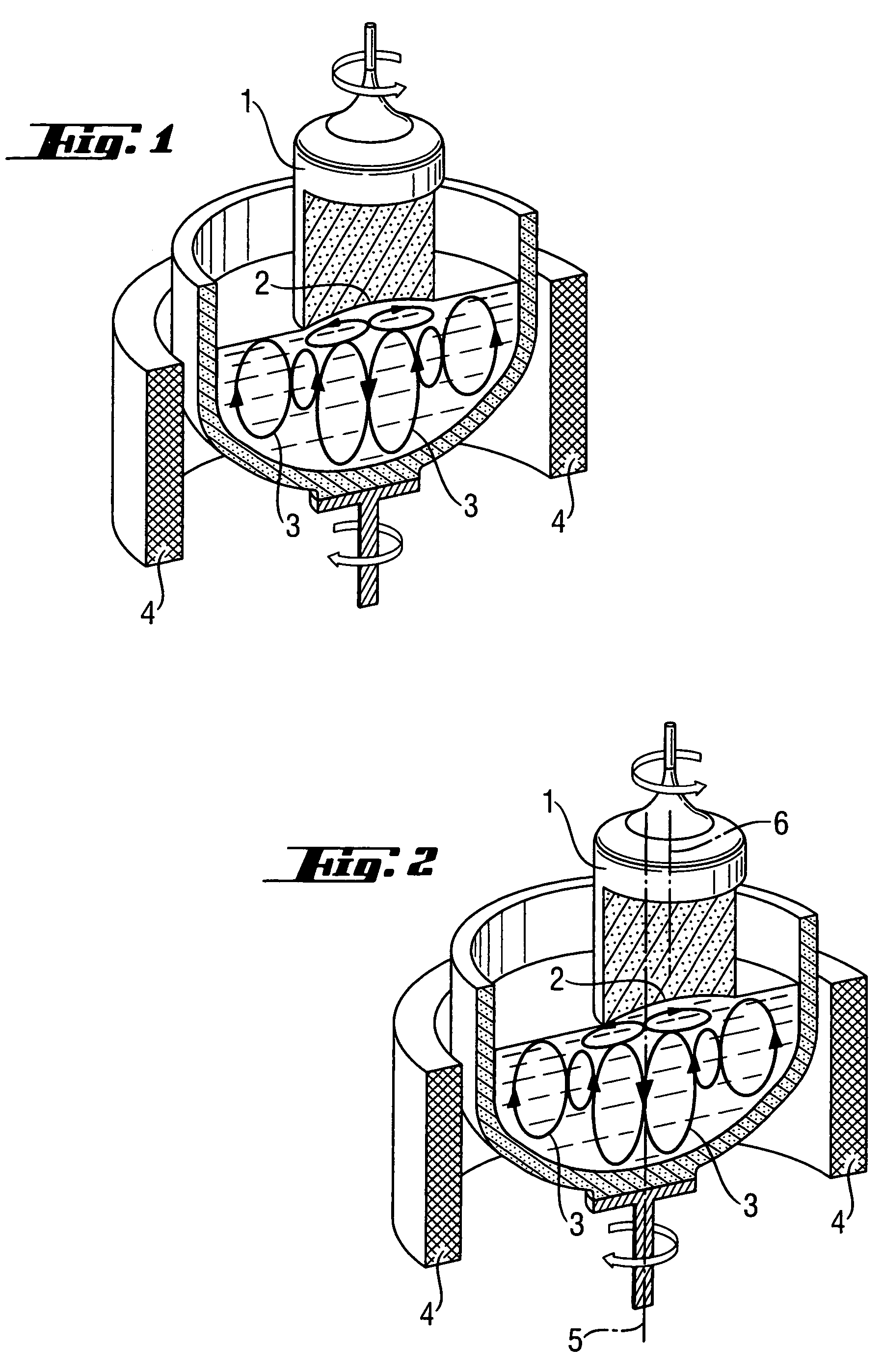
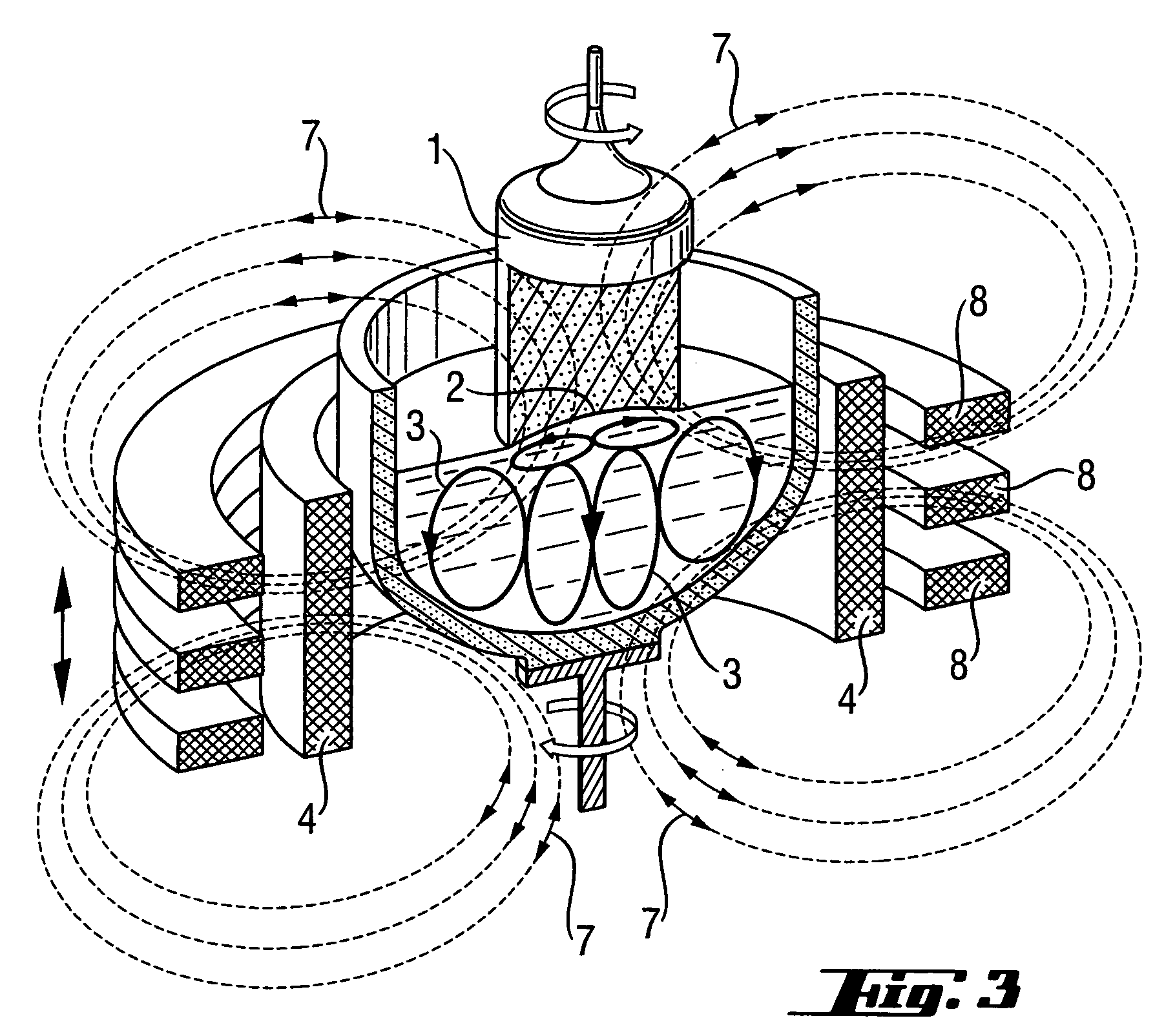
[0044]FIG. 6 shows an axial longitudinal section through a single crystal which has been pulled under conventional conditions using a rotationally symmetrical traveling magnetic field, corresponding to the arrangement illustrated in FIG. 3. The strongly curved radial profile of the solidification interface 11 can be seen very clearly from lifetime measurements (μPCD) as illustrated in longitudinal section. For comparison purposes, FIG. 7 presents a lifetime measurement which clearly reveals the effect of partially shielding a traveling magnetic field. During production of the crystal, an arrangement with an asymmetric traveling field (ATMF), as diagrammatically illustrated in FIG. 4, was used, with otherwise identical crystal pulling conditions. Compared to FIG. 6, the lifetime measured on a longitudinal section throu...


PUM

PropertyMeasurementUnit
diameteraaaaaaaaaa
diameteraaaaaaaaaa
diametersaaaaaaaaaa

Abstract

A silicon single crystal which, over an ingot length of over 10 percent of the total ingot length, has a uniform defect picture and narrow radial dopant and oxygen variations. The process in accordance with the Czochralski method involves bringing about a temperature distribution in the melt in the region of the solidification interface which deviates from rotational symmetry.

Description

[0001]This application is a division of and claims priority to U.S. patent application Ser. No. 10 / 732,119 filed Dec. 10, 2003 now abandoned, and also claims priority to German Application DE 102 59 588.7 filed Dec. 19, 2002.BACKGROUND OF THE INVENTION[0002]1. Field of the Invention[0003]The present invention relates to a silicon single crystal and to a process for producing it, in which the single crystal is pulled from a melt using the Czochralski method. This method has long been known and is used on an industrial scale to produce semiconductor wafers which in turn form the base material for the fabrication of electronic components.[0004]2. The Prior Art[0005]It is also known that the production of single crystals which have a diameter of 200 mm or greater imposes particular demands. In particular, there are considerable difficulties with deliberately setting the radial crystal properties within the narrowest possible range. This is true in particular for the concentration of for...

Claims


Application Information

Patent Timeline
Patent Type & Authority Patents(United States)
IPC IPC(8): C30B15/20C30B15/00C30B15/14C30B29/06
CPCC30B15/14C30B15/203C30B29/06C30B15/206Y10T117/1068Y10S117/917C30B15/00
Inventor WEBER, MARTINVON AMMON, WILFRIEDSCHMIDT, HERBERTVIRBULIS, JANISGELFGAT, YURIGORBUNOV, LEONID
Owner SILTRONIC AG
Why Eureka
Try Eureka