
High-speed router with backplane using tuned-impedance thru-holes and vias

a high-speed router and tuned-impedance technology, applied in the field of backplanes, can solve the problems of extreme performance and drive up the cost, and achieve the effects of reducing complexity, shortening the length of the longest loop, and reducing the number of differential pairs

Active Publication Date: 2008-02-26
DELL MARKETING CORP
View PDF40 Cites 25 Cited by
  • Summary
  • Abstract
  • Description
  • Claims
  • Application Information

AI Technical Summary

Benefits of technology

[0005]The preferred embodiments described in the '622 application incorporate a number of unconventional design features, such as a high layer count (and large overall thickness), thick power planes, and an exotic dielectric material. While these backplanes are capable of throughputs measurable in Terabits / second and high-wattage, low-noise power distribution, the features used to obtain this extreme performance tend to drive up cost.
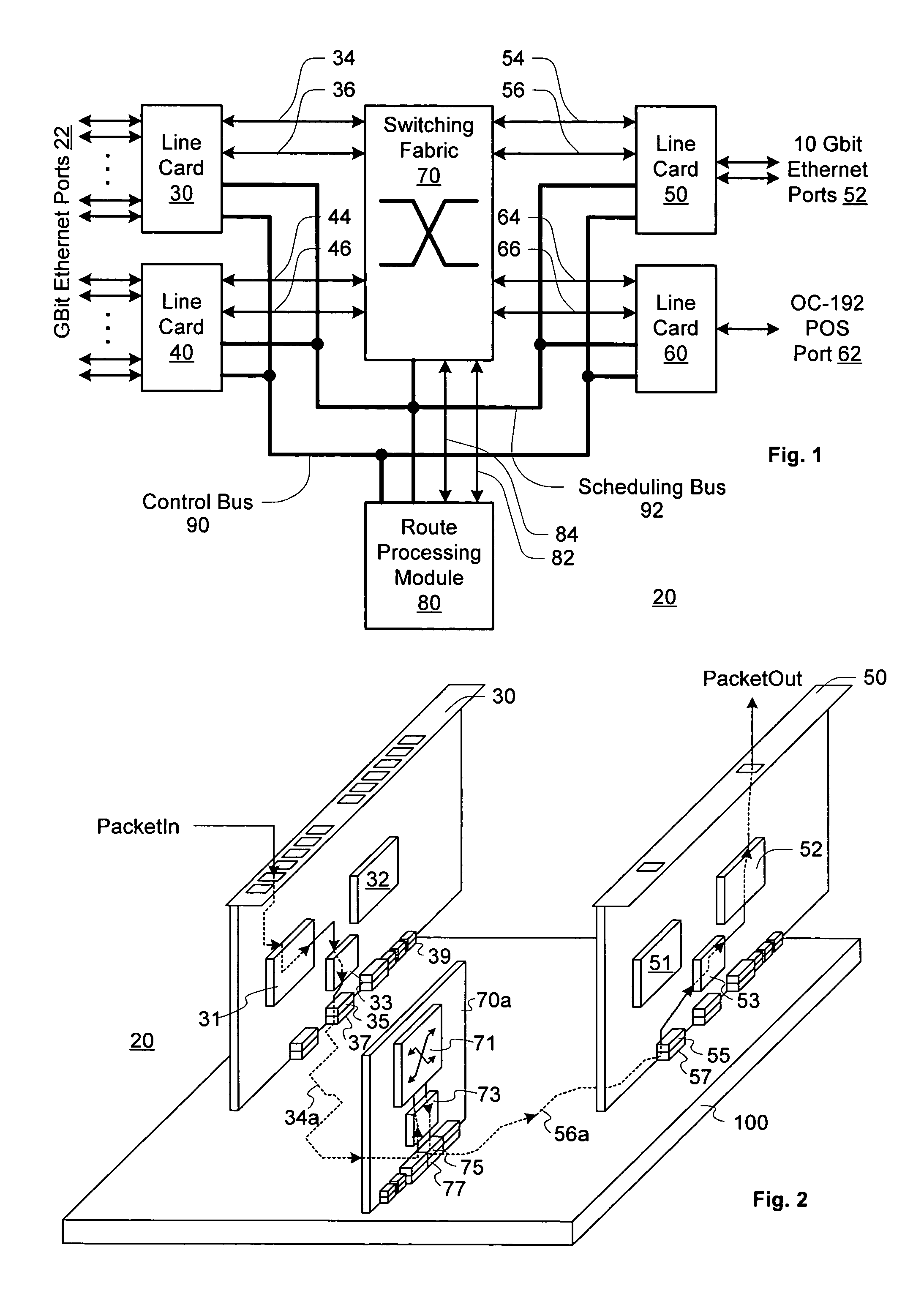
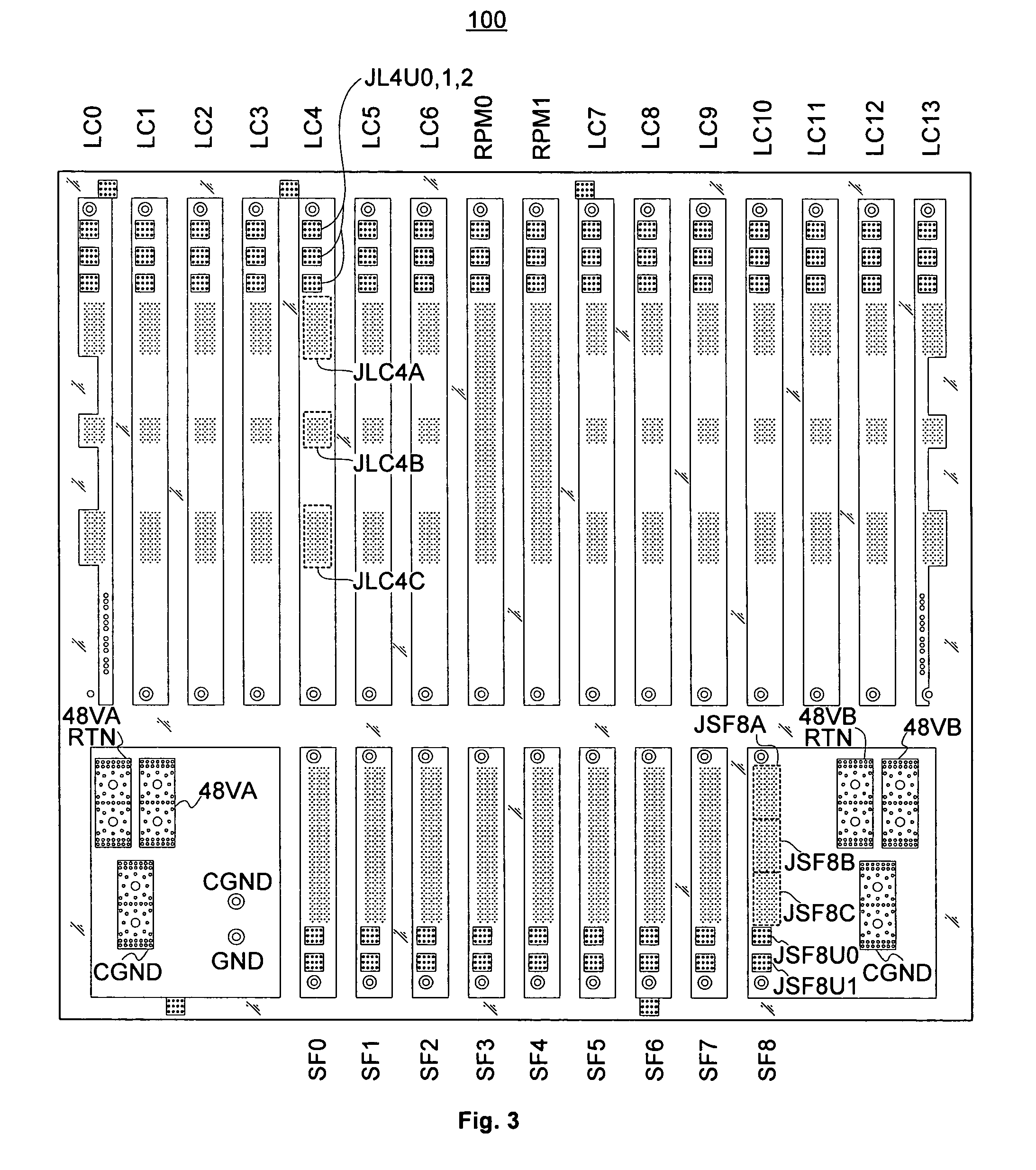
[0006]In some applications, the router described in the prior application uses only a fraction of the available backplane card slots and massive bandwidth. It has now been recognized that a need exists for a smaller, simpler, and more economic backplane that retains most of the desirable qualities of the full-feature backplane. Consequently, some of the embodiments described herein seek to support the same line, switch fabric, and RPM card types as described for the full-feature backplane, but in a backplane (and router) form factor with significantly decreased complexity.
[0007]In one embodiment, the maximum number of line cards supported has been reduced from fourteen to seven, and the maximum signaling speed has been reduced to 3.125 Gbps. This allows for a different layout with shorter longest-trace lengths, smaller differential pairs, thinner power planes, and a much thinner board with significantly fewer signal layers (four vs. fourteen layers for the larger board). It has also been discovered that, at least for 3.125 Gbps operation, this embodiment can be fabricated entirely using FR4 insulating material instead of more exotic materials such as N6000.
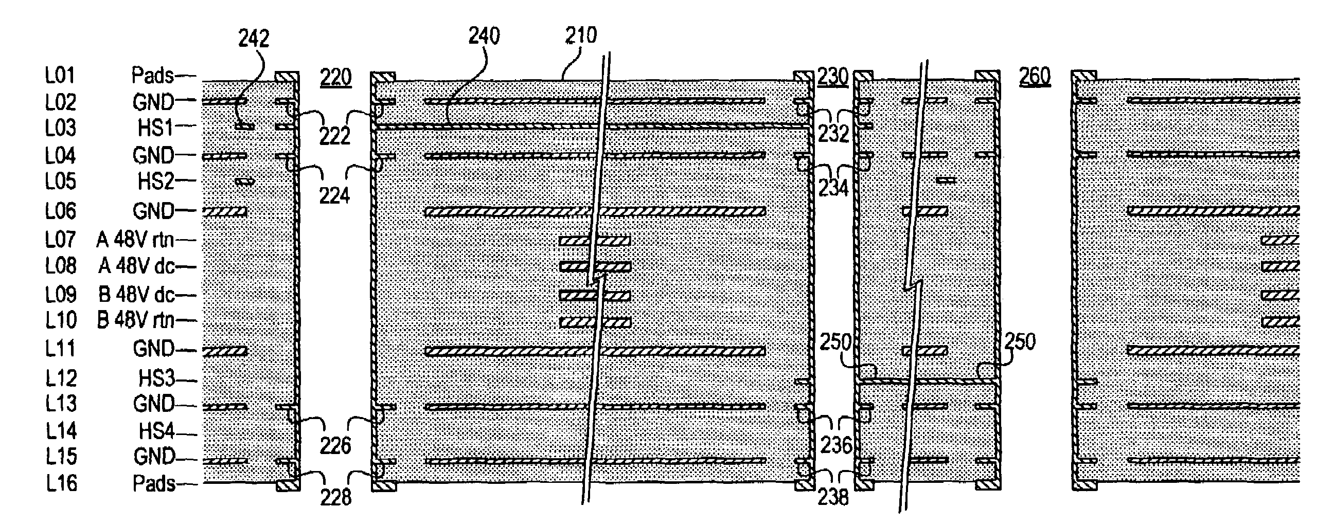
[0008]Even with the reduction in trace count due to supporting half as many line cards, this embodiment would be considerably thicker were it not for one other significant difference from the prior design—it incorporates layer-swapping vias. It has been found that the additional signal degradation created by passing signals thru vias can be largely compensated for by the use of nonfunctional pads to alter the impedance of the vias.

Problems solved by technology

While these backplanes are capable of throughputs measurable in Terabits / second and high-wattage, low-noise power distribution, the features used to obtain this extreme performance tend to drive up cost.

Method used


Image

  • High-speed router with backplane using tuned-impedance thru-holes and vias
  • High-speed router with backplane using tuned-impedance thru-holes and vias
  • High-speed router with backplane using tuned-impedance thru-holes and vias

Examples


Embodiment Construction

[0019]Several terms have been assigned particular meanings within the context of this disclosure. As used herein, high speed signaling refers to signaling on a differential signal pair at a data rate greater than about 2.5 Gbps. A high-speed signaling layer or high-speed differential trace plane contains high-speed differential signal trace pairs, but may also contain lower speed and / or single-ended traces. A core dielectric layer is one that is cured and plated prior to assembly of a circuit board. A b-stage dielectric layer is one that is cured during assembly of cores into the circuit board. Differential signaling (or balanced signaling) is a mode of signal transmission, using two conductors, in which each conductor carries a signal of equal magnitude, but, opposite polarity. Single-ended signaling (or unbalanced signaling) is a mode of signal transmission where one conductor carries a signal with respect to a common ground. The impedance of a differential trace is more different...


PUM


Abstract

A high-speed router backplane is disclosed. The router backplane uses differential signal pairs on multiple signal layers, each sandwiched between a pair of digital ground layers. To reduce routing complexity, at least some of the differential signal pairs route through a via pair, somewhere along their path, to a different signal layer. Specific via designs reduce differential signal distortion due to the via pair, allowing the backplane to operate reliably at differential signal rates in excess of 3 Gigabits per second. In particular, each via passes through nonfunctional conductive pads on selected digital ground plane layers, the pads separated from the remainder of its ground plane layer by a clearance, thereby modifying the impedance of the via and reducing reflections from the stubs created by the via.

Description

FIELD OF THE INVENTION[0001]This invention relates generally to backplanes, and more specifically to backplane wiring systems for highly interconnected, high-speed modular digital communications systems such as routers and switches.BACKGROUND OF THE INVENTION[0002]A backplane generally comprises a printed circuit board having a number of card connection slots or bays. Each slot or bay comprises, e.g., one or more modular signal connectors or card edge connectors, mounted on the backplane. A removable circuit board or “card” can be plugged into the connector(s) of each slot. Each removable circuit board contains drivers and receivers necessary for communication of signals across the backplane with corresponding drivers and receivers on other removable circuit boards.[0003]One or more layers of conductive traces are formed on and / or in the backplane. The traces connect to individual signal connection points at the various slots to form data lines and control lines.[0004]In U.S. patent...

Claims


Application Information

Patent Timeline
IPC IPC(8): H01R12/16
CPCH05K1/0251H05K1/116H05K1/0245H05K3/429H05K2201/044H05K2201/09236H05K2201/09454H05K2201/09636H05K2201/09781
Inventor GOERGEN, JOEL R.
Owner DELL MARKETING CORP
Learn More