

System and method for providing a highly efficient wide bandwidth power supply for a power amplifier
- Summary
- Abstract
- Description
- Claims
- Application Information
AI Technical Summary
Benefits of technology
Problems solved by technology
Method used
Image

Examples
Embodiment Construction
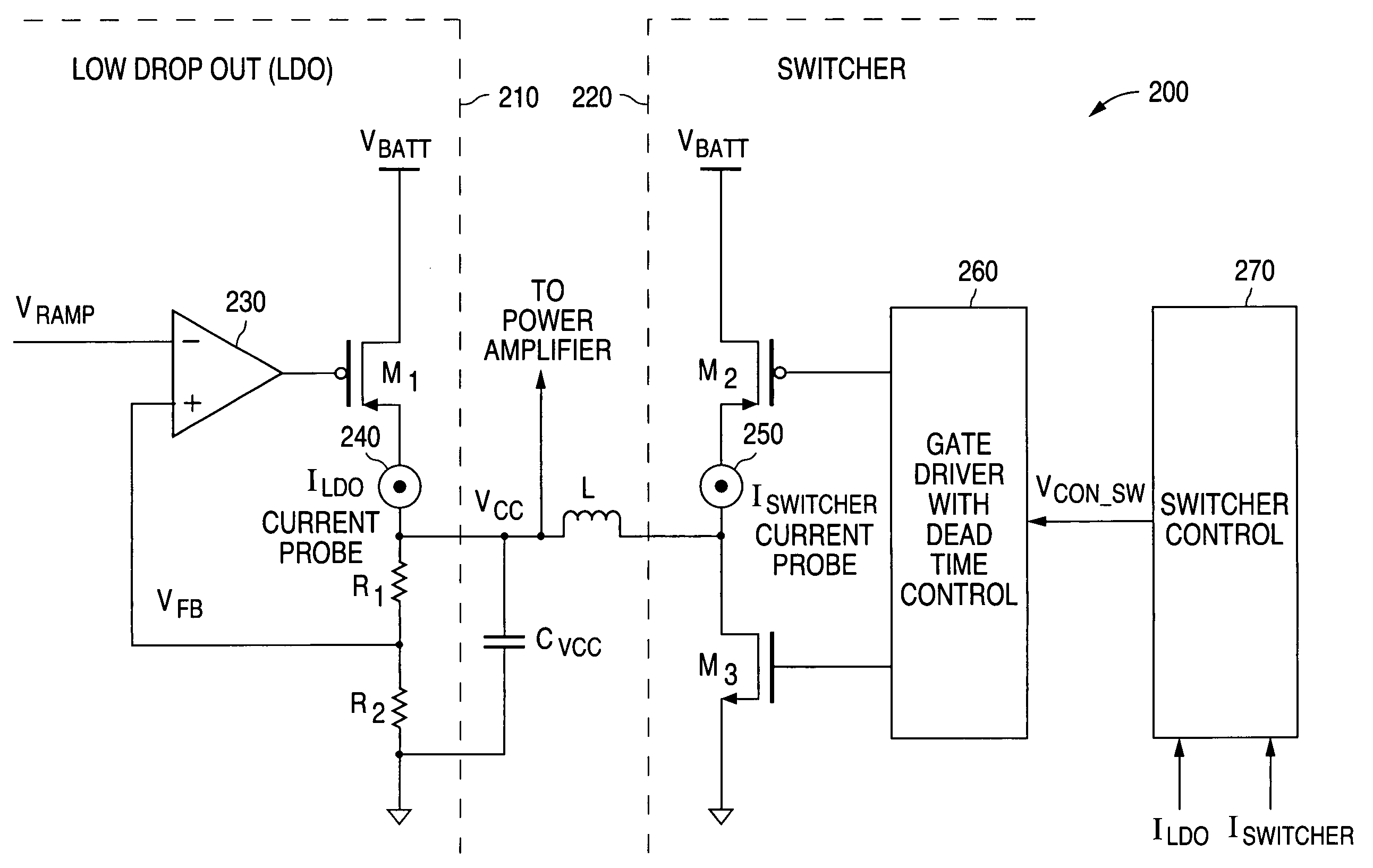
[0035]FIGS. 1 through 9 and the various embodiments used to describe the principles of the present invention in this patent document are by way of illustration only and should not be construed in any way to limit the scope of the invention. Those skilled in the art will understand that the principles of the present invention may be implemented in any type of suitably arranged power amplifier circuit.
[0036]To simplify the drawings the reference numerals from previous drawings will sometimes not be repeated for structures that have already been identified.
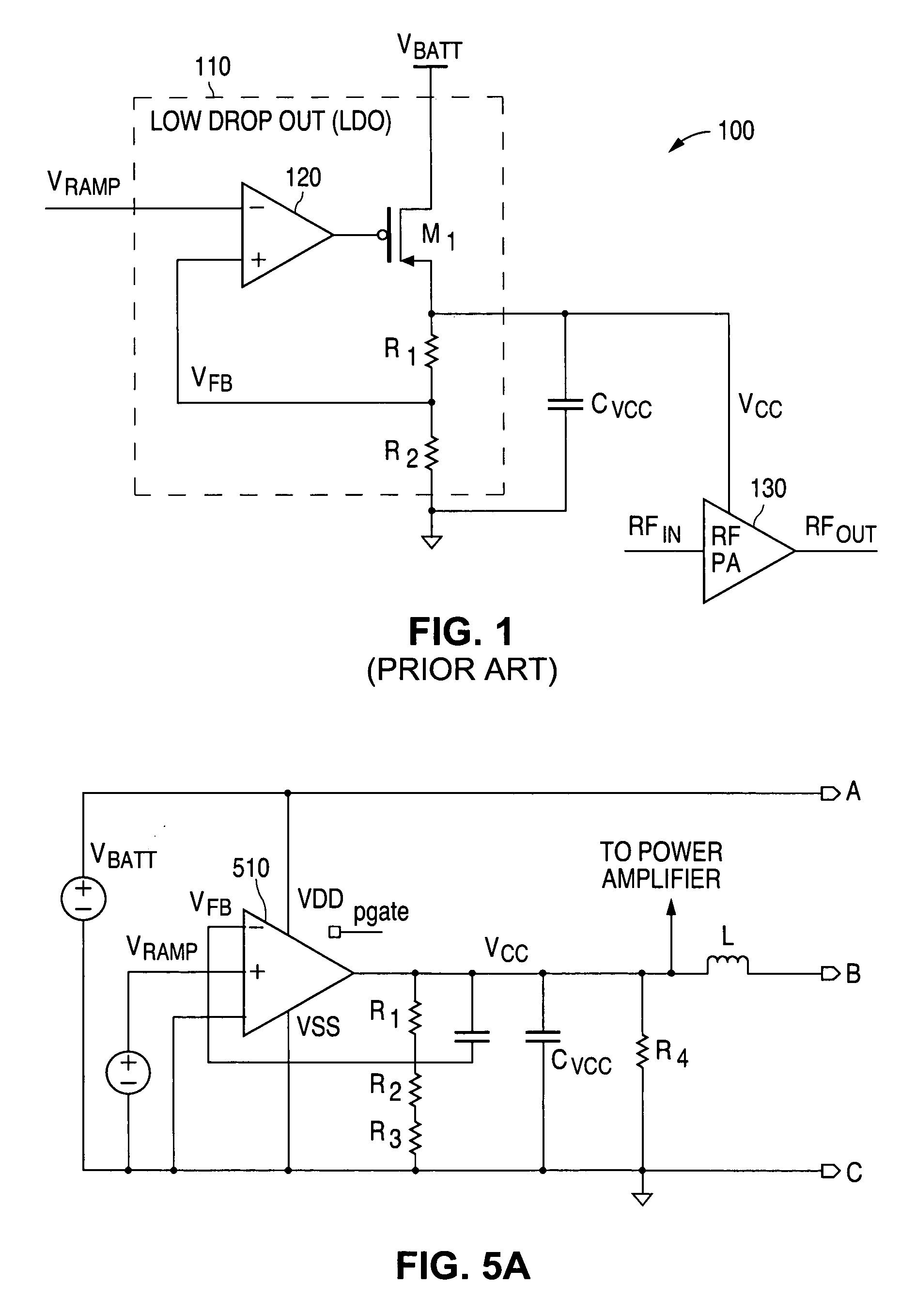
[0037]FIG. 1 illustrates a schematic diagram of a prior art power supply control circuit 100. Power supply control circuit 100 comprises a low drop out (LDO) circuit 110. Low drop out (LDO) circuit 110 comprises an operational amplifier 120 that receives a Vramp signal on its inverting input. A feedback voltage signal VFB is provided to the non-inverting input of operational amplifier 120. The operating voltage for low drop out (LDO)...
PUM
 Abstract
Description
Claims
Application Information