Process for manufacturing a composite polymeric circuit protection device

a protection device and polymer technology, applied in the direction of resistor housing/enclosement/embedding, positive temperature coefficient thermistors, printed element electric connection formation, etc., can solve the problem of tedious process, and achieve the effect of simple device build-up and inexpensive mass production

Inactive Publication Date: 2008-03-18
LITTELFUSE INC
View PDF124 Cites 11 Cited by
  • Summary
  • Abstract
  • Description
  • Claims
  • Application Information

AI Technical Summary

Benefits of technology

[0007]As described in copending, commonly assigned U.S. patent application Ser. No. 09 / 060,278 (Chiang et al, filed Apr. 14, 1998), now U.S. Pat. No. 6,606,023 (issued Aug. 12, 2003). the disclosure of which is incorporated herein by reference, composite devices can be prepared by sorting individual devices and then assembling the sorted devices into composite devices. Such a process can be tedious, as it may require that the resistance of each individual device be read. We have now found, in accordance with the present invention, that it is possible to prepare a multilayer assembly from which individual composite devices can be divided. Such an assembly allows preparation of a large number of composite devices simultaneously. Furthermore, because the process described herein allows the patterning of individual layers of the assembly before or after fabrication into the assembly, a variety of different devices can be prepared from the same starting layers. In addition, the composition of the layers can be easily varied, allowing the simple build-up of devices with combined functionality. Various interconnection schemes between layers can be simply implemented, and devices with multiple external electrical contacts can be made without changing the basic manufacturing process. All of these further add to the broad range of different devices which can be inexpensively mass-produced by the process disclosed herein.
[0008]This invention provides methods and processes for which various operative steps can be carried out on an assembly which will yield a plurality of devices when subdivided into composite devices by subdividing along both x- and y-directions (where x and y correspond to directions in the plane of the laminar PTC elements). The ability to prepare devices in this way is a significant improvement over other methods, for example that described in U.S. application Ser. No. 09 / 060,278 (now U.S. Pat. No. 6,606,023), because for this invention, individual devices do not need to be individually assembled, increasing the efficiency and therefore reducing the cost of the manufacturing process. Finally, the method of combiining layers of materials to form composite devices disclosed herein allows an extremely simple yet adaptable method for forming a variety of devices without the necessity of changing the basic manufacturing process.

Problems solved by technology

Such a process can be tedious, as it may require that the resistance of each individual device be read.

Method used


Image

  • Process for manufacturing a composite polymeric circuit protection device
  • Process for manufacturing a composite polymeric circuit protection device
  • Process for manufacturing a composite polymeric circuit protection device

Examples


example

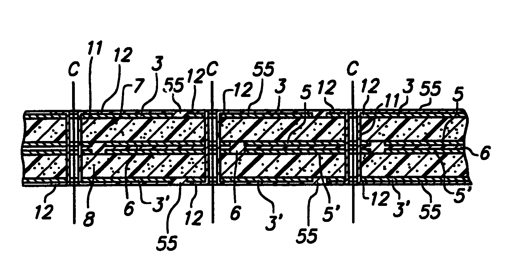
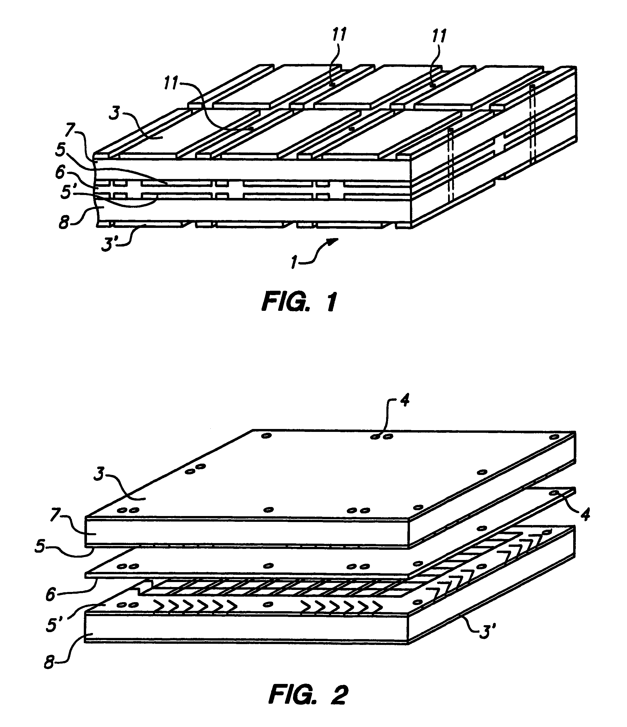
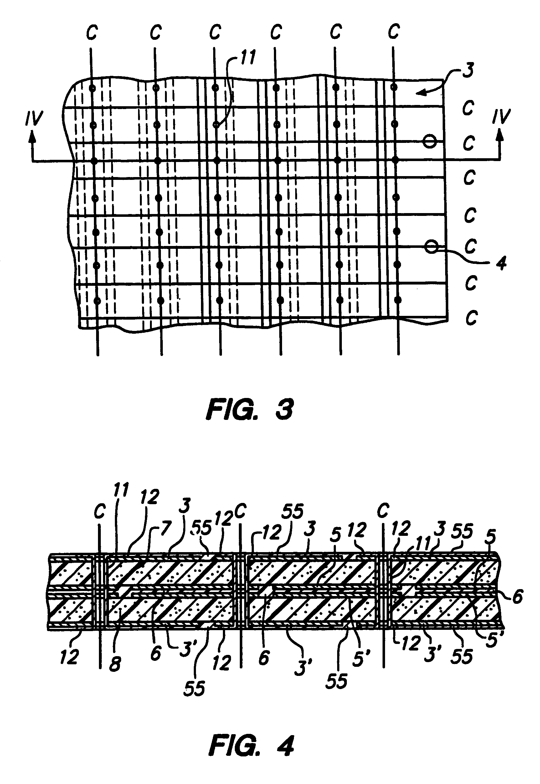
[0114]A stack in accordance with FIGS. 1 and 2 was prepared by the following method. Two laminates, each having a thickness of about 0.264 mm (0.0104 inch) were prepared by attaching a nickel / copper foil having a thickness of about 0.0356 mm (0.0014 inch) to both sides of a 0.193 mm (0.0076 inch)-thick sheet of conductive polymer. The conductive polymer was prepared by mixing about 40% by volume carbon black (Raven™ 430, available from Columbian Chemicals) with about 60% by volume high density polyethylene (Chevron™ 9659, available from Chevron), and then extruding into sheet and laminating in a continuous process. The laminated sheet was cut into individual laminates of 0.30 m×0.41 m (12 inch×16 inch). The laminates were irradiated to 4.5 Mrad using a 4.5 MeV electron beam.

[0115]Each of the laminates was drilled in an asymmetric pattern around its the periphery to provide holes and slots to register the laminates in a known x-y orientation in the plane of the laminate. These regist...


PUM

PropertyMeasurementUnit
resistanceaaaaaaaaaa

Abstract

A process for manufacturing a composite polymeric circuit protection device in which a polymeric assembly is provided and is then subdivided into individual devices. The assembly is made by providing first and second laminates, each of which includes a laminar polymer element having at least one conductive surface, providing a pattern on at least one of the conductive surfaces on one laminate, securing the laminates in a stack in a desired configuration, at least one conductive surface of at least one of the laminates forming an external conductive surface of the stack, and making a plurality of electrical connections between a conductive surface of the first laminate and a conductive surface of the second laminate. The laminar polymer elements may be PTC conductive polymer compositions, so that the individual devices made by the process exhibit PTC behavior.

Description

CROSS-REFERENCE TO RELATED APPLICATIONS[0001]This application is a continuation of commonly assigned Application Ser. No. 09 / 395,869, filed Sep. 14, 1999 now U.S. Pat. No. 6,640,420 the disclosure of which is incorporated herein by reference.BACKGROUND OF THE INVENTION[0002]1. Field of the Invention[0003]This invention relates to electrical devices and assemblies and methods of making such devices and assemblies.[0004]2. Introduction to the Invention[0005]Circuit protection devices comprising a conductive polymer composition having a positive temperature coefficient (PTC) are well-known. Such devices which are intended for surface mounting onto a substrate, e.g. a printed circuit board, are disclosed in U.S. Pat. Nos. 5,831,510 (Zhang et al), 5,852,397 (Chan et al), and 5,864,281 (Zhang et al), International Publications Nos. 94 / 01876 (Raychem Corporation) and 95 / 08176 (Raychem Corporation), and copending, commonly assigned Application Ser. No. 09 / 181,028 (Graves et al, filed Oct. 2...

Claims


Application Information

Patent Timeline
Patent Type & Authority Patents(United States)
IPC IPC(8): H01C17/00H01C1/14H01C7/02H01C7/18H01C13/02H05K3/00H05K3/40
CPCH01C1/1406H01C7/027H01C7/18H01C13/02H01C17/006H01C7/021Y10T29/49083H05K3/0052H05K3/403Y10T29/49101Y10T156/1092Y10T29/49085Y10T29/49105Y10T29/49098Y10T29/49082Y10T29/49091Y10T29/49128
Inventor HETHERTON, SCOTTMONTOYA, WAYNEBRUGUIER, THOMASDAERING, RANDY
Owner LITTELFUSE INC
Why Eureka
Try Eureka