Functional timing analysis for characterization of virtual component blocks

a virtual component and timing analysis technology, applied in the field of electronic circuit design automation, can solve the problems of limiting their applicability, requiring unacceptably large computation resources for larger circuit designs, and increasing complexity, and achieve the effect of simplifying timing characterization of virtual component blocks or circuit models

Inactive Publication Date: 2008-03-18
CADENCE DESIGN SYST INC
View PDF13 Cites 1 Cited by
  • Summary
  • Abstract
  • Description
  • Claims
  • Application Information

AI Technical Summary

Benefits of technology

[0020]The invention provides in one aspect systems and methods for performing a timing analysis on virtual component blocks or other circuit models by using functional information obtained from the circuit's control inputs and their useful combinations. A useful technique for condensing time delay information (whether scalar or tabular in form) is also provided, to simplify timing characterization of a virtual component block or circuit model.

Problems solved by technology

However, they both have the disadvantage that their complexity increases exponentially with circuit size, limiting their applicability, or requiring unacceptably large amounts of computation resources for larger circuit designs.
A drawback with such timing analysis methods is that they suffer from delay underestimation.
Delay underestimation is a serious problem in circuit design because it can lead to incorrect operation.
A computational advantage of this condition is that it depends only on the final (stable) values of the inputs and is independent of the input event times. However, a drawback of static sensitization techniques is that, if the two inputs of a gate are controlling, they incorrectly assume that the paths from both inputs are false.
A big disadvantage is its failure to detect any false paths, leading to overly pessimistic results.

Method used


Image

  • Functional timing analysis for characterization of virtual component blocks
  • Functional timing analysis for characterization of virtual component blocks
  • Functional timing analysis for characterization of virtual component blocks

Examples


Embodiment Construction

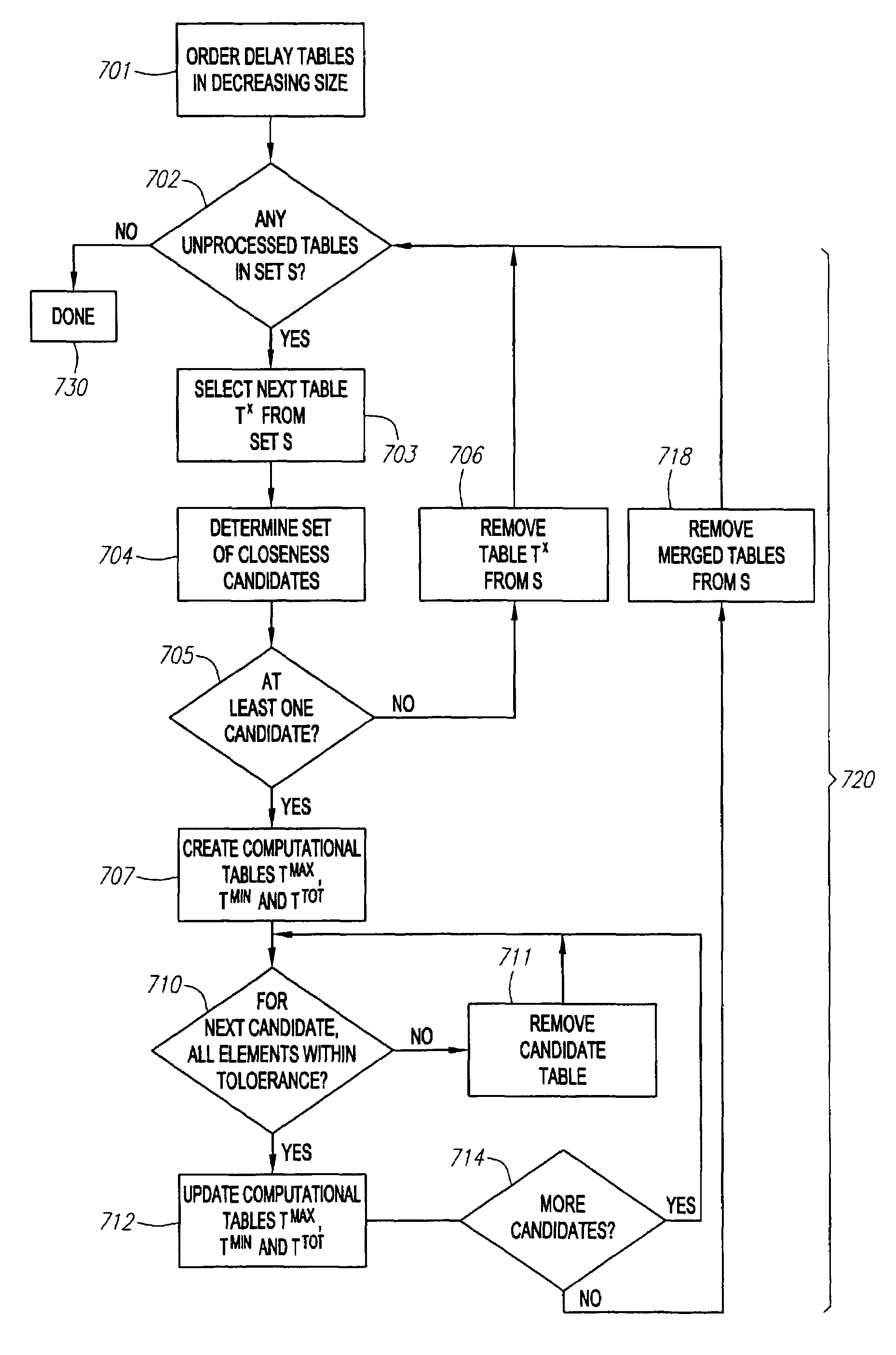
[0035]In one or more embodiments as disclosed herein, a system and method are provided for performing a timing analysis on virtual component blocks by using functional information obtained from the circuit's control inputs and their useful combinations. A preferred technique for performing timing analysis is illustrated by a process flow diagram 600 in FIG. 6, and may be explained with reference to the various other figures from time to time.

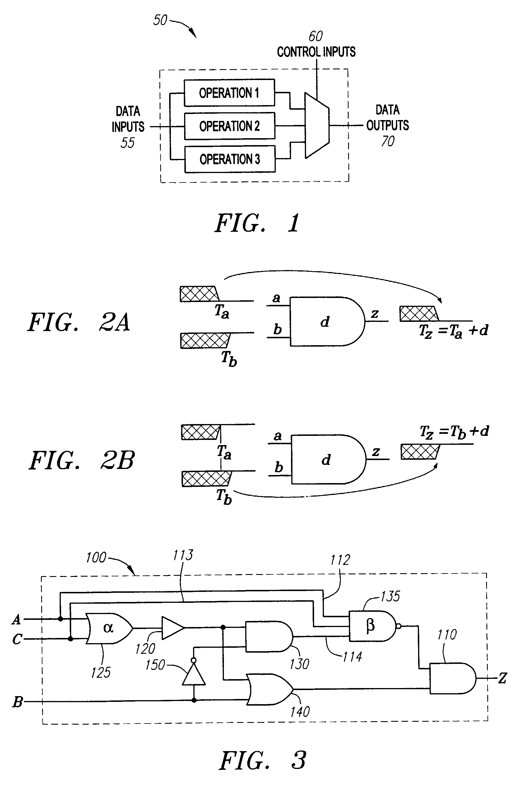
[0036]According to the embodiment illustrated in FIG. 6, as a first step 601 in the timing analysis flow diagram 600 depicted therein, the set of inputs for a given virtual component block is divided by the circuit designer into data inputs and control inputs. The division of circuit inputs into data inputs and control inputs is a task commonly performed by circuit designers, and is considered well within the purview of those skilled in the art. An example of a simple circuit showing control inputs 70 and data inputs 55 is illustrated in FIG. 1 ...


PUM


Abstract

A system and method for performing a timing analysis on virtual component blocks or other circuit models is provided wherein functional information obtained from the circuit's control inputs and their useful combinations is used to improve accuracy. The control inputs and data inputs for a circuit block are identified. Each functionally meaningful or useful control input combination is applied to the circuit block, and the topological delay for the data inputs are determined only along the paths that are not blocked by the control inputs. The delays along paths that are blocked are ignored. The analysis is further augmented by determining the topological delay for all paths originating at control inputs, without regard to blocking of paths, so as to reduce the chance for possible underestimation of delays from the data inputs. A final timing model may include the combination of maximum delays along data paths for each combination of control inputs, and maximum delays along paths originating from each of the control inputs. The delay analysis may account for different input slews and load capacitances, and the results may be expressed in tabular or matrix form. A useful technique for condensing time delay information (whether scalar or tabular in form) is also provided, to simplify timing characterization of a virtual component block or circuit model. Delay tables or matrixes that are “close” (i.e., within a specified tolerance) may be combined into a single table or matrix.

Description

RELATED APPLICATIONS DATA[0001]This application is a continuation of U.S. patent application Ser. No. 09 / 477,710, filed Dec. 28, 1999, now U.S. Pat. No. 6,457,159, which claims priority of U.S. Provisional Application Ser. No. 60 / 114,253, filed on Dec. 29, 1998, the entirety of which is incorporated by reference herein.FIELD OF THE INVENTION[0002]The field of the present invention relates to electronic design automation and, more particularly, to methods and systems for timing analysis of electronic circuit blocks.BACKGROUND OF THE INVENTION[0003]Advances in silicon technology increasingly allow larger and more complex designs to be formed on a single chip. Designs may consist of millions or tens of millions of transistors on a single chip. At the same time, however, market demands continue to push designers to develop designs more rapidly and efficiently. A recent trend to increase design speed and efficiency involves the re-use or recycling of electronic circuit blocks or subsyste...

Claims


Application Information

Patent Timeline
Patent Type & Authority Patents(United States)
IPC IPC(8): G06F9/45G06F17/50
CPCG06F17/5022G06F30/33
Inventor YALCIN, HAKANPALMERO, ROBERT J.SAKALLAH, KAREM A.MORTAZAVI, MOHAMMAD S.BAMJI, CYRUS
Owner CADENCE DESIGN SYST INC
Why Eureka
Try Eureka