Integrated implementation of a collector boost scheme and method therefor

a collector boost and boost scheme technology, applied in the field of amplifiers, can solve the problems of not being realized in a low-cost integrated power amplifier, not being demonstrated in a practical fashion, and requiring a much more complex power supply than the dc-to-dc converter approach, so as to improve the linearity of the power amplifier

Active Publication Date: 2008-03-25
SIGE SEMICON
View PDF10 Cites 67 Cited by
  • Summary
  • Abstract
  • Description
  • Claims
  • Application Information

AI Technical Summary

Benefits of technology

[0012]In accordance with the invention there is provided a method of improving linearity of a power amplifier comprising: amplifying an RF signal to provide an amplified RF signal comprising: providing an amplifier circuit including an amplifier voltage input port; in a first mode of operation, providing a first voltage potential to the amplifier voltage input port; in a second other mode of operation, providing a boosted voltage potential to the amplifier voltage input port, the boosted voltage potential formed by summing a first voltage potential from a voltage supply and a second voltage potential stored within a capacitor; and, switching from the first mode to the second mode in dependence upon a detected a presence of a peak pulse within the RF signal.

Problems solved by technology

Linearity requirements, however, force the gain / phase response to be linear with voltage change, or that pre-distortion is applied.
Envelope tracking requires an even more complex power supply than the DC-to-DC converter approach and has yet to be demonstrated in a practical fashion.
However, the disadvantage of such a circuit is that it is not realizable within a low cost integrated power amplifier due to the difficulty in integrating the inductor and the PA on the same substrate.

Method used


Image

  • Integrated implementation of a collector boost scheme and method therefor
  • Integrated implementation of a collector boost scheme and method therefor
  • Integrated implementation of a collector boost scheme and method therefor

Examples


Embodiment Construction

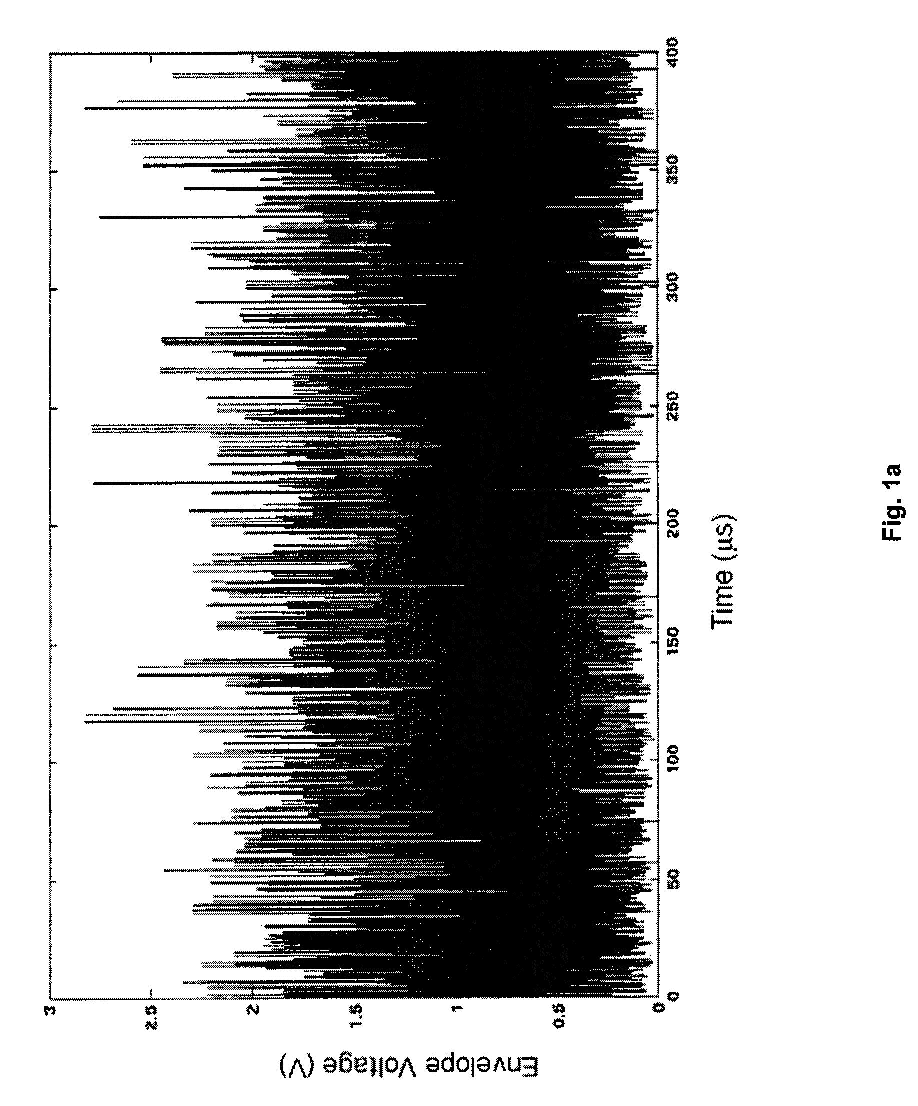
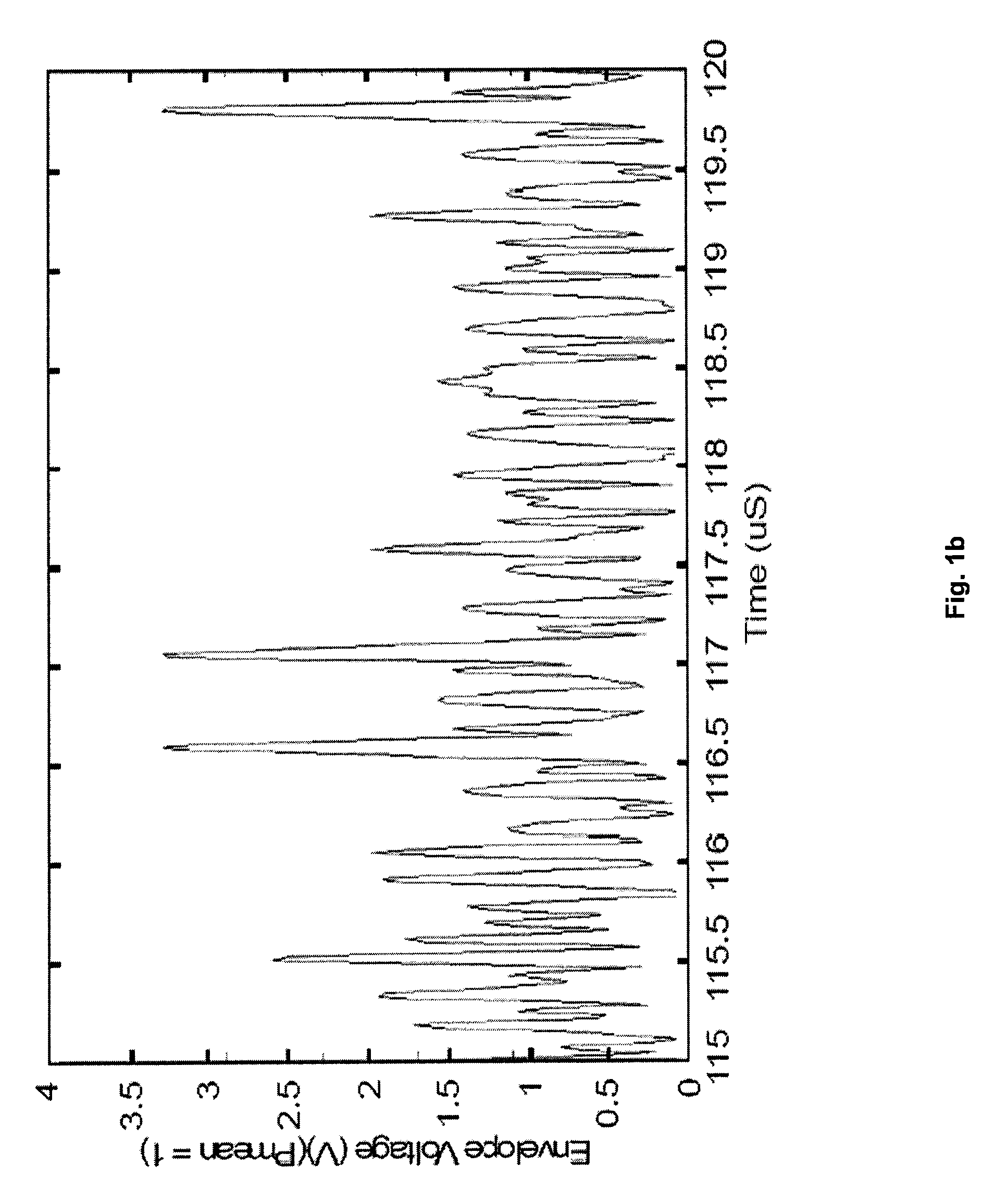
[0025]Referring to FIG. 1a, a graph of linear RF output voltage versus time for 100 OFDM symbols is shown. The graph represents the magnitude of the RF envelope. In an ideal system, power used in the power amplifier (PA) would be at any instant proportional to the square of the RF voltage required. The peaks of the signal occur infrequently thus the mean output power of the PA is significantly below its peak output. So even in a class B amplifying stage where the current used is proportional to signal amplitude the constant dc collector supply voltage has to be toleranced to handle the peaks of the signal without amplifier clipping. This results in inefficiency when the amplifier is operating at lower power levels since there is unused voltage headroom available to the amplifier. If a lower supply voltage is used the amplifier distorts on the peaks and the information content of the OFDM signal may be jeopardised.

[0026]Current generation portable battery operated devices rely on adv...


PUM


Abstract

A collector boost circuit is disclosed for providing a first voltage in a first mode of operation to a power amplifier, and a second voltage in a second mode of operation to the power amplifier. The collector boost circuit uses a switch and an indicator signal for triggering the switch between the first and the second mode of operation. The second voltage is a boosted voltage greater than the first voltage and is provided during peak excursions through a boost capacitor.

Description

FIELD OF THE INVENTION[0001]The invention relates to amplifiers and more particularly to integrated power amplifiers.BACKGROUND OF THE INVENTION[0002]Frequency division multiplexing (FDM) is a technology for transmitting different data sets within each of multiple signals simultaneously over a single transmission path, such as a cable or wireless system. Each signal travels within a carrier—a unique frequency range that is modulated by data being transmitted.[0003]Orthogonal frequency division multiplexing (OFDM) is a spread spectrum technique that distributes each data set of the different data sets over a large number of carriers that are spaced apart at predetermined frequencies. This spacing provides the “orthogonality” in this technique, which allows for demodulators that are responsive only to frequencies relating to a signal data set. The benefits of OFDM are high spectral efficiency, resiliency to RF interference, and lower multi-path distortion. OFDM is advantageous because...

Claims


Application Information

Patent Timeline
Patent Type & Authority Patents(United States)
IPC IPC(8): H03F3/04
CPCH03F1/0211H03F3/24H03F3/345H03F3/70
Inventor WHITTAKER, EDWARD J. W.
Owner SIGE SEMICON
Why Eureka
Try Eureka