
Method of flexible clock placement for integrated circuit designs using integer linear programming

a technology of integrated circuits and programming methods, applied in the field of integrated circuits, can solve the problems of significant device area, requiring a substantial amount of operating power, and the clock placement problem is believed to be an np-complete problem, and achieve the effect of minimizing the total number of physical clock regions and minimizing the physical clock regions

Active Publication Date: 2008-04-01
XILINX INC
View PDF4 Cites 7 Cited by
  • Summary
  • Abstract
  • Description
  • Claims
  • Application Information

AI Technical Summary

Benefits of technology

[0013]The method can include defining at least one virtual clock region which comprises at least one physical clock region, wherein the ILP formulation minimizes physical clock regions included within each virtual clock region. Each virtual clock region can be mapped to 0 or more of the plurality of physical clock regions if a feasible clock placement exists for the circuit design. In another embodiment, the specifying step can include defining the ILP formulation to depend upon an objective function comprising a sum of a first and a second function. The first function can minimize a total number of physical clock regions and the second function can minimize virtual clock regions used by global clock networks of the circuit design. The second function can include a coefficient which regulates distribution of global clock networks among the plurality of physical clock regions of the PLD.
[0015]The objective function can depend upon a sum of a first and a second function. The first function can minimize the sum of the physical clock regions of the PLD within each virtual clock region of the circuit design. The second function can minimize a sum of virtual clock regions used by global clock networks of the circuit design. The method also can include mapping each virtual clock region to zero or more physical clock regions of a set of physical clock regions for the PLD if a feasible clock placement exists for the circuit design.

Problems solved by technology

Global clock trees require a significant amount of device area, or silicon, to implement and also require a substantial amount of operating power in the field.
In consequence, most FPGAs include a limited number of global clock trees.
The clock placement problem is believed to be an NP-Complete problem.
Both approaches, however, are non-exact and often fail to produce a feasible solution for the clock placement problem.
In consequence, PLD designers usually perform a manual floor-planning for the circuit design, which is cumbersome and time-consuming.
With designs continuing to utilize larger numbers of global clock networks, clock placement is likely to become a hindrance to rapid circuit design.

Method used


Image

  • Method of flexible clock placement for integrated circuit designs using integer linear programming
  • Method of flexible clock placement for integrated circuit designs using integer linear programming
  • Method of flexible clock placement for integrated circuit designs using integer linear programming

Examples


Embodiment Construction

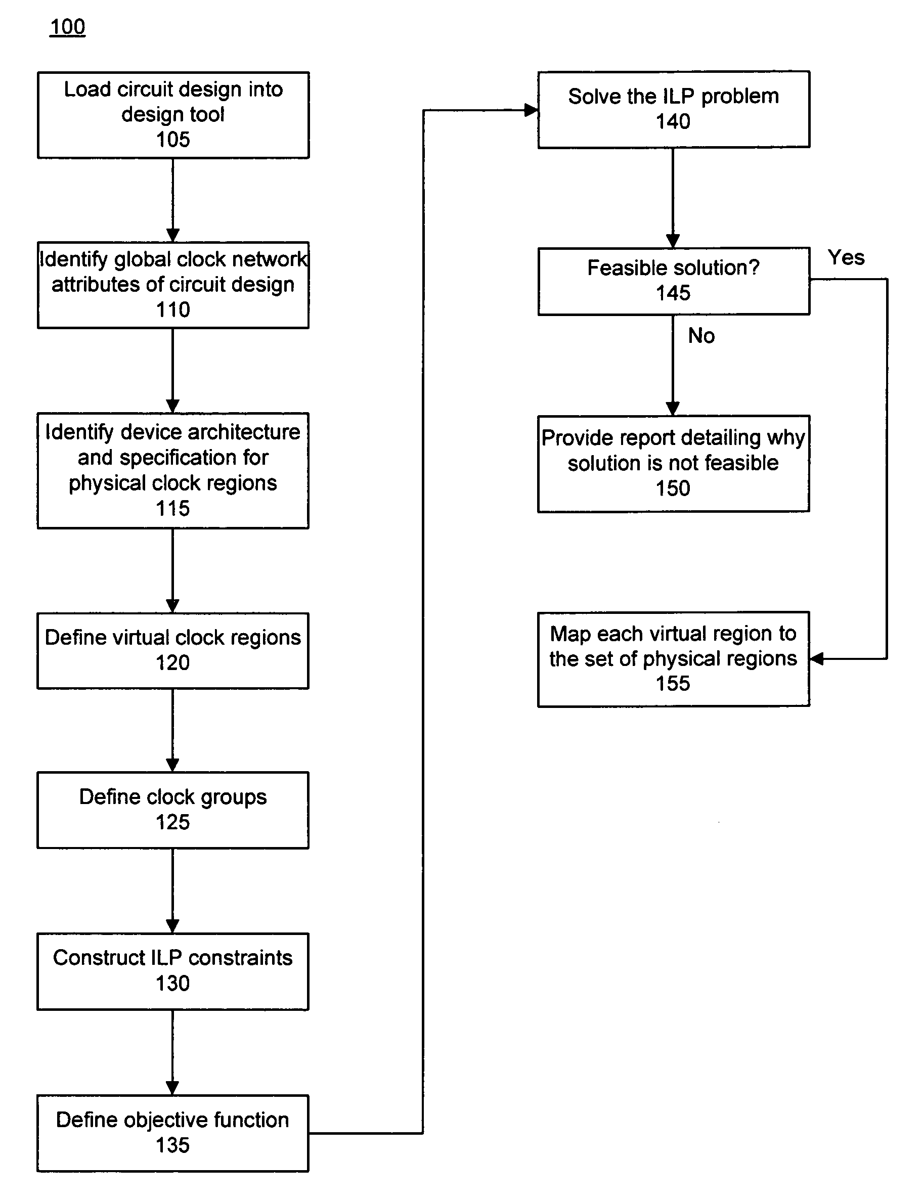
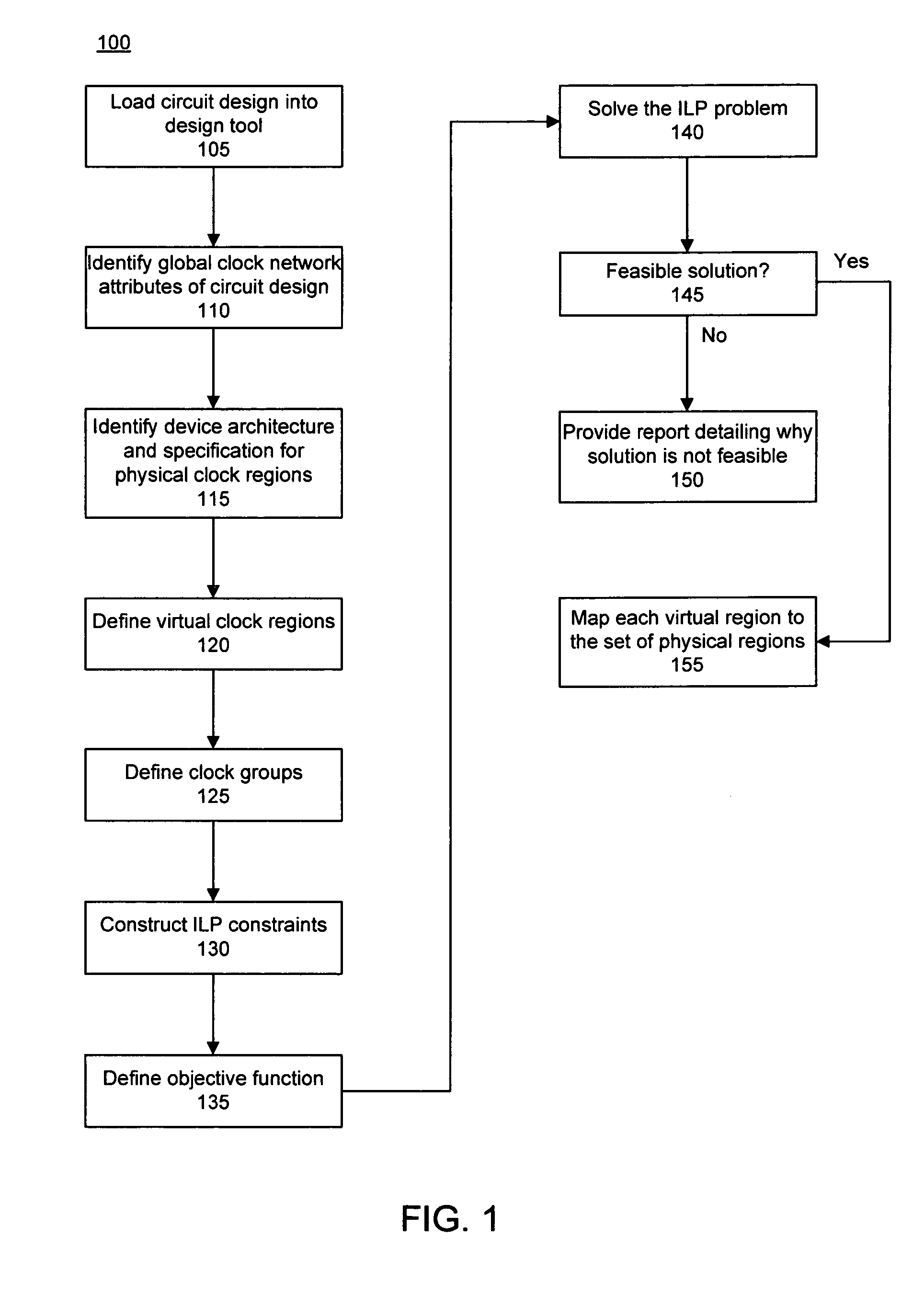
[0030]The present invention provides methods for placing global clocks within programmable logic devices (PLDs). In accordance with the present invention, Integer Linear Programming (ILP) is used to formulate a potential solution to the clock placement problem for a given circuit design. More particularly, the feasibility of the clock placement problem can be determined for a given circuit design. The feasibility of the clock placement problem can be determined in light of any defined constraints, particularly those relating to compatibility and / or capacity of the PLD in which the circuit design is to be implemented. If clock placement is feasible, a valid assignment of global clock networks to clock regions can be determined for the circuit design.

[0031]FIG. 1 is a flow chart illustrating a method 100 of determining the feasibility of clock placement for a circuit design and for determining clock region assignments in accordance with the inventive arrangements disclosed herein. In ...


PUM


Abstract

A method of global clock placement for a circuit design to be implemented on a programmable logic device (PLD) can include identifying clock properties for the circuit design and identifying physical clock region attributes for the PLD. The method further can include specifying an Integer Linear Programming formulation (ILP) of a clock placement problem for the circuit design from the clock properties and the physical clock region attributes. The ILP formulation can be solved to determine whether a feasible clock placement exists for the circuit design.

Description

BACKGROUND[0001]1. Field of the Invention[0002]This invention relates to the field of integrated circuits and, more particularly, to the allocation of global clock networks to physical clock regions of a programmable logic device.[0003]2. Description of the Related Art[0004]Modern programmable logic devices (PLDs), and particularly field programmable gate arrays (FPGAs), utilize a plurality of optimized global clock trees. Global clock trees also can be referred to as differential global clock trees, global clock lines, matched skew global clock lines, global clock interconnects, global clock network resources, or global clock spines. In any case, these global clock trees are responsible for reliably clocking sequential logic components of the PLD. Global clock trees require a significant amount of device area, or silicon, to implement and also require a substantial amount of operating power in the field. In consequence, most FPGAs include a limited number of global clock trees. The...

Claims


Application Information

Patent Timeline
IPC IPC(8): G06F17/50
CPCG06F17/5054G06F17/5072G06F2217/62G06F30/34G06F30/392G06F30/396G06F30/343
Inventor KANNAN, PARIVALLALSLONIM, VICTOR Z.ABID, SALIM
Owner XILINX INC
Learn More