DAC cell circuit

Active Publication Date: 2005-01-18
MEDIATEK INC
View PDF8 Cites 11 Cited by
  • Summary
  • Abstract
  • Description
  • Claims
  • Application Information

AI Technical Summary

Benefits of technology

In view of the above-mentioned problems, the invention provides a DAC cell circuit, which is capable of quickly settling the output current using control signals without non-overlap timing control. Also, the DAC cell

Problems solved by technology

However, when the operation frequency of the microprocessor is getting higher, the demands for the precision and speed of the DAC are getting stricter.
The unnecessary error circuit operation makes the transistor 11 be turned off.
This may limit the operation sp

Method used


Image

  • DAC cell circuit
  • DAC cell circuit
  • DAC cell circuit

Examples


Embodiment Construction

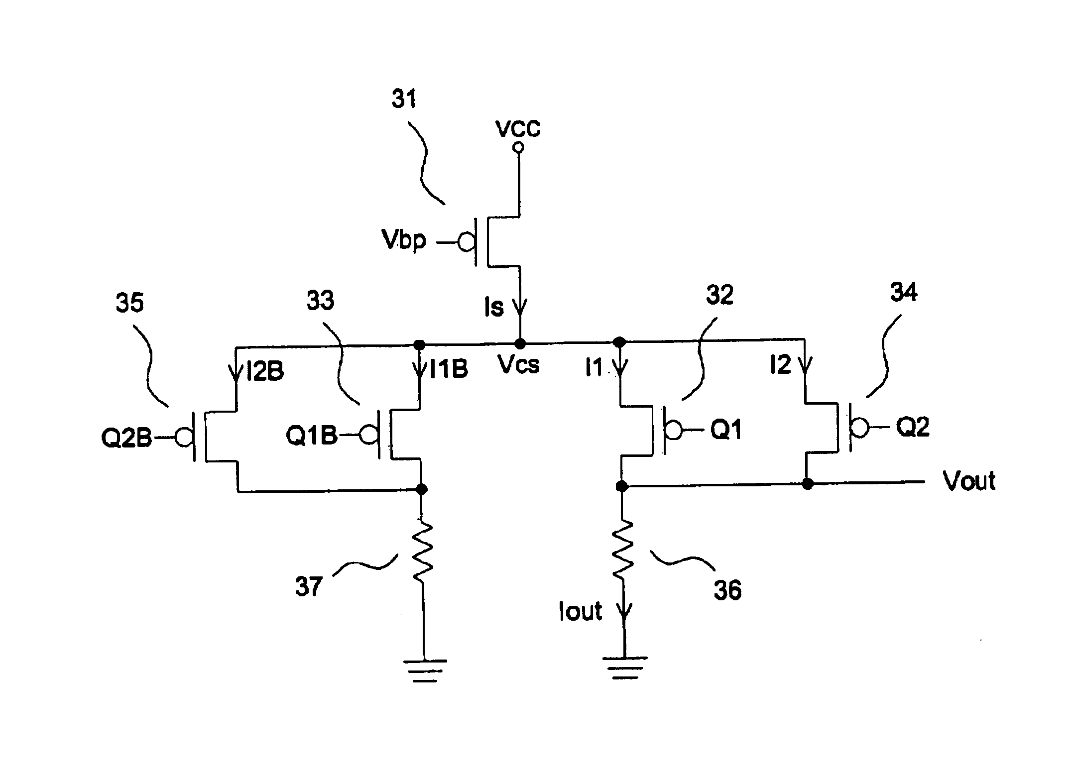
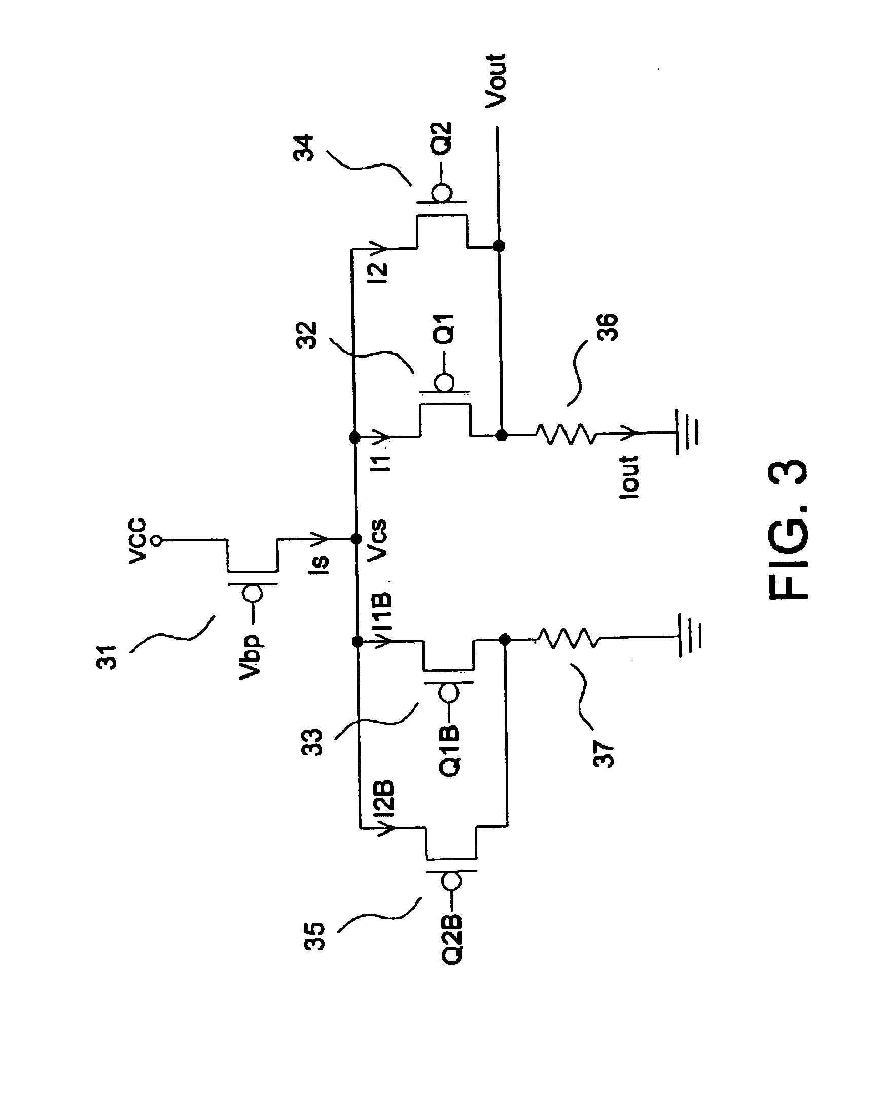
FIG. 3 shows a DAC cell circuit according to the present invention. As shown in FIG. 3, the DAC cell circuit includes a PMOSFET 31 and a set of PMOSFETs 32, 33, 34 and 35. The PMOSFET 31 is controlled by a signal Vbp with constant voltage and serves as a constant current source to provide a constant current for the DAC cell circuit. The PMOSFETs 32 to 35 serve as 2 pairs of current switches, wherein the four PMOSFETs are transistors having the same dimension. The sources of the PMOSFETs 32 to 35 are all connected to the drain of the PMOSFET 31, and the drains of the PMOSFETs 32 to 35 are connected to a pair of resistors 36 and 37. The switching operations of the PMOSFETs 32 to 35 are controlled by control signals Q1, Q1B, Q2 and Q2B, which are respectively input to the gates of the PMOSFETs 32 to 35. The control signals Q1, Q1B, Q2 and Q2B are a set of control signals with delay timing control. As shown in FIG. 4, the control signal Q2 is a delayed control signal of the control sign...


PUM


Abstract

A digital-analog converter (DAC) cell circuit. The circuit includes a current source, a first resistor, a second resistor, a first MOSFET, a second MOSFET, a third MOSFET and a forth MOSFET. The first MOSFET has a source and a drain connected to the current source and the first resistor, respectively, and a gate receiving a first control signal. The second MOSFET has a source and a drain connected to the current source and the second resistor, respectively, and a gate receiving a second control signal. The third MOSFET has a source and a drain connected to the source and drain of the first MOSFET, respectively, and a gate receiving a third control signal. The fourth MOSFET has a source and a drain connected to the source and drain of the second MOSFET, respectively, and a gate receiving a fourth control signal. The third control signal is a signal delayed of the first signal and the forth control signal is a signal delayed of the second signal. The delayed control signal can be used to control the slew rate of current DAC cell, thus reduce the package inductance induced L di/dt noise. Also it can be used to reduce the voltage fluctuations during current switching so as to get fast settling current.

Description

BACKGROUND OF THE INVENTION1. Field of the InventionThe invention relates to a semiconductor integrated circuit, and more particularly, to a current DAC (Digital-Analog Converter) cell circuit, which can reduce the voltage fluctuations during current switching so as to make the output voltage reaching stable quickly. Also we can reduce the current spike when large current switching instantaneously by controlling the slew rate of output current.2. Description of the Related ArtRecently, owing to the enhancing efficiency of the microprocessor for the personal computer, the demands for image processing are getting higher. Consequently, the digital-to-analog converters (DACs) are getting more important for the image display. However, when the operation frequency of the microprocessor is getting higher, the demands for the precision and speed of the DAC are getting stricter. It is quite important to perform digital-to-analog conversion with fast settling and high accuracy.FIG. 1 is a con...

Claims


Application Information

Patent Timeline
IPC IPC(8): H03M1/06H03M1/08H03M1/74
CPCH03M1/0678H03M1/742H03M1/0863
Inventor KAO, HSUEH-WU
Owner MEDIATEK INC
Why Eureka
Try Eureka