Multi-chamber MOCVD growth apparatus for high performance/high throughput

a mocvd growth and multi-chamber technology, applied in the direction of crystal growth process, polycrystalline material growth, chemically reactive gas, etc., can solve the problems of complex doping control, memory effects of earlier growth steps where dopants have been intentionally introduced, and can be limited, so as to achieve the effect of reducing or eliminating the growth stop

Active Publication Date: 2008-05-06
CREE INC
View PDF26 Cites 53 Cited by
  • Summary
  • Abstract
  • Description
  • Claims
  • Application Information

AI Technical Summary

Benefits of technology

[0011]In one embodiment the present invention is a method of conducting multiple step multiple chamber chemical vapor deposition while avoiding reactant memory in the relevant reaction chambers. The method includes depositing a layer of semiconductor material on a substrate using vapor deposition in a first deposition chamber followed by evacuation of the growth chamber to reduce vapor deposition source gases remaining in the first deposition chamber after the deposition growth and prior to opening the chamber. The substrate is transferred to a second deposition chamber while isolating the first deposition chamber from the second deposition chamber to prevent reactants present in the first chamber from affecting deposition in the second chamber and while maintaining an ambient that minimizes or eliminates growth stop effects. After the transferring step, an additional layer of a different semiconductor material is deposited on the first deposited layer in the second chamber using vapor deposition.
[0012]In a second embodiment, the invention is a method of conducting multiple step multiple semiconductor chemical vapor deposition while avoiding reactant memory in the relevant reaction chambers. The method includes depositing a layer of a first semiconductor material on a substrate using vapor deposition in a first deposition chamber, followed by evacuation of the growth chamber to reduce vapor deposition source gases remaining in the first deposition chamber following the deposition growth and prior to opening the chamber. The substrate is transferred to a second deposition chamber while isolating the first deposition chamber from the second deposition chamber to prevent reactants present in the first chamber from affecting deposition in the second chamber and while maintaining an ambient that minimizes or eliminates growth stop effects. After the transferring step, a second layer of a different semiconductor material is deposited on the substrate in the second chamber using vapor deposition. After the second layer is deposited and prior to opening the second deposition chamber, the vapor deposition source gases are evacuated from the second deposition chamber to reduce vapor deposition source gases remaining in the second deposition chamber following the deposition growth and the substrate is transferred to the first deposition chamber while isolating the second deposition chamber from the first deposition chamber to prevent reactants present in the second chamber from affecting deposition in the first deposition chamber and while maintaining an ambient that minimizes or eliminates growth stop effects. After the transferring step, an additional layer of the first semiconductor material is deposited on the second deposited layer in the first chamber using vapor deposition.

Problems solved by technology

Such changes in source or dopant gas composition can lead to a problem referred to as “reactant memory.” The term “reactant memory” describes the undesired contamination of the process gas with source or dopant compositions or elements that remain in the chamber from previous deposition steps.
Doping control is intricate in the epitaxial growth procedure.
The background doping can be limited by using purified gases, and high-grade materials in the critical parts of the reactor.
Memory effects from earlier growth steps where dopants have been intentionally introduced are also problematic.
These solutions, however, suffer from several drawbacks.
Each method is time-consuming and reduces output, and adds additional processing steps to the technique.
These methods may also result in growth stop effects such as poor adhesion between layers.
Moreover, the various proposed solutions to the problem of reactant memory can also be costly additions to production of the desired devices.
Reactant memory has not, however, been sufficiently reduced using these techniques to allow for efficient low doping epitaxial growth of multiple layers in some processes.

Method used


Image

  • Multi-chamber MOCVD growth apparatus for high performance/high throughput
  • Multi-chamber MOCVD growth apparatus for high performance/high throughput
  • Multi-chamber MOCVD growth apparatus for high performance/high throughput

Examples


Embodiment Construction

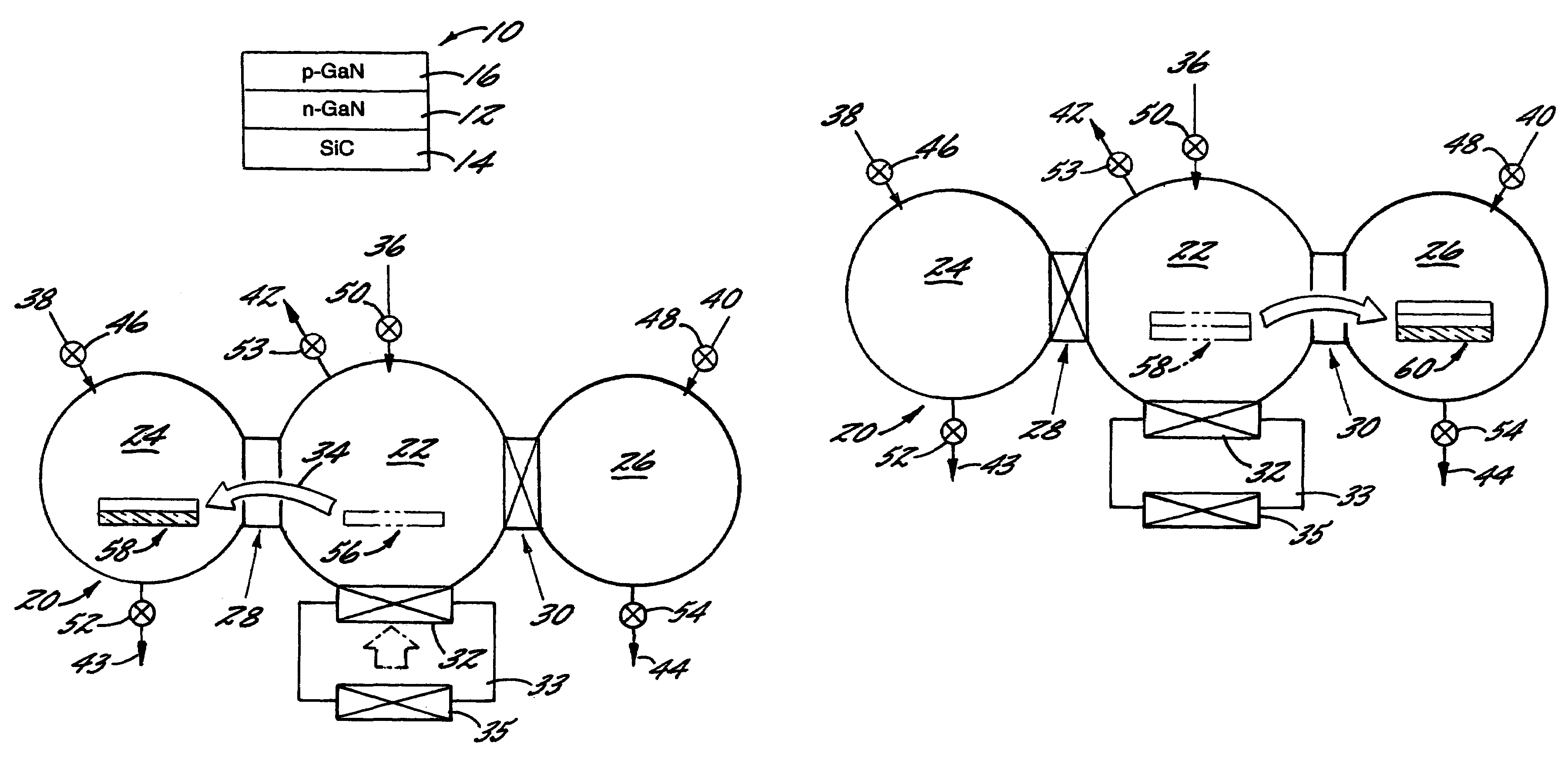
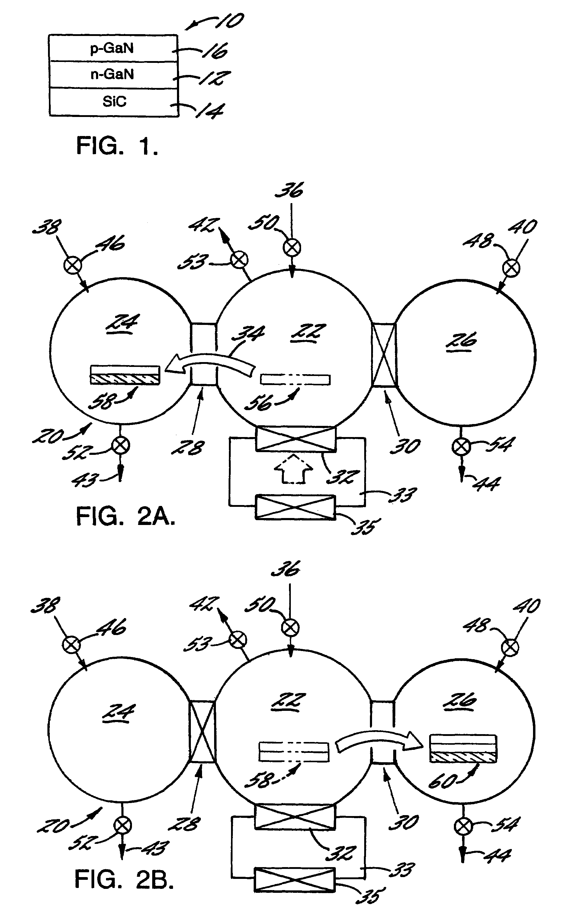
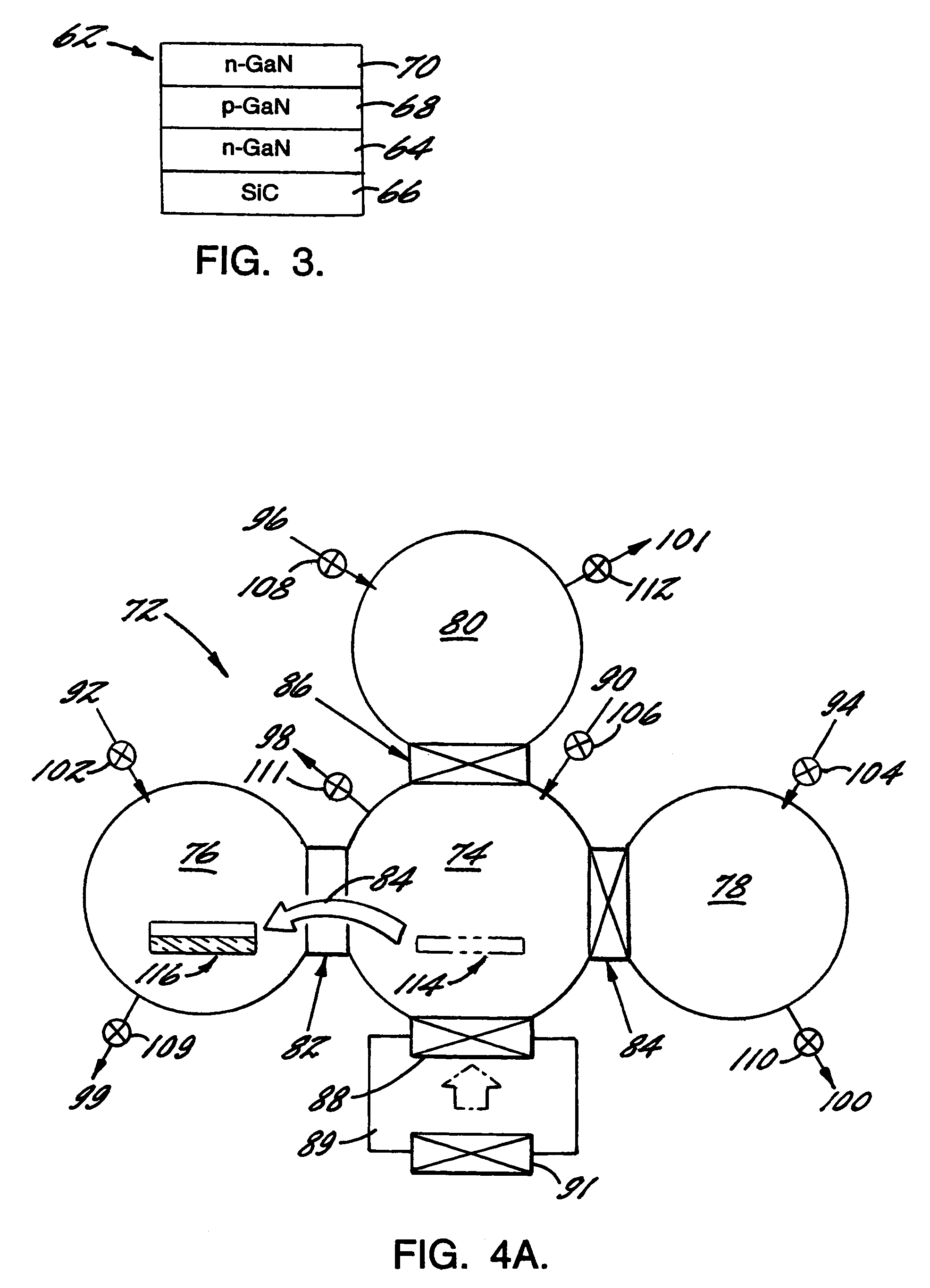
[0020]The present invention now will be described more fully hereinafter with reference to the accompanying drawings, in which preferred embodiments of the invention are shown. This invention may, however, be embodied in many different forms and should not be construed as limited to the embodiments set forth herein; rather, these embodiments are provided so that this disclosure will be thorough and complete, and will fully convey the scope of the invention to those skilled in the art. In the drawings, the thickness of layers and regions are exaggerated for clarity. It will be understood that when an element such as a layer, region or substrate is referred to as being “on” another element, it can be directly on the other element or intervening elements may also be present. In contrast, when an element is referred to as being “directly on” another element, there are no intervening elements present. It will also be understood that references to a “wafer” includes one wafer as well as m...


PUM

PropertyMeasurementUnit
semiconductoraaaaaaaaaa
n-type conductivityaaaaaaaaaa
temperatureaaaaaaaaaa

Abstract

In one embodiment the present invention is a method of conducting multiple step multiple chamber chemical vapor deposition while avoiding reactant memory in the relevant reaction chambers. The method includes depositing a layer of semiconductor material on a substrate using vapor deposition in a first deposition chamber followed by evacuation of the growth chamber to reduce vapor deposition source gases remaining in the first deposition chamber after the deposition growth and prior to opening the chamber. The substrate is transferred to a second deposition chamber while isolating the first deposition chamber from the second deposition chamber to prevent reactants present in the first chamber from affecting deposition in the second chamber and while maintaining an ambient that minimizes or eliminates growth stop effects. After the transferring step, an additional layer of a different semiconductor material is deposited on the first deposited layer in the second chamber using vapor deposition.

Description

BACKGROUND OF THE INVENTION[0001]The present invention is related to vapor deposition growth of semiconductor materials and to associated apparatus and methods. More specifically, the present invention is related to a wafer processing apparatus and a wafer processing method for reducing reactant memory in the relevant apparatus chambers.[0002]Crystal growth from vapor is employed in semiconductor technology, in particular, for producing epitaxial layers on semiconductor wafers. The term epitaxy typically describes the growth of a monocrystalline layer on the planar boundary surface of a monocrystalline substrate, generally a substrate wafer of a semiconductor material.[0003]Epitaxial growth is often carried out using chemical vapor deposition (CVD) in CVD reactors. In such processes, the semiconductor wafer is first heated and then exposed to a gas mixture, referred to as a process gas. The process gas mixture typically consists of a source gas, a carrier gas, and, where appropriate...

Claims


Application Information

Patent Timeline
Patent Type & Authority Patents(United States)
IPC IPC(8): H01L21/00
CPCC23C16/4408C30B25/08C30B29/40C30B29/403C30B29/406H01L21/0237H01L21/02378H01L21/02458H01L21/02502H01L21/0254H01L21/02543H01L21/02546H01L21/02576H01L21/02579H01L21/0262C23C16/54Y10T29/41
Inventor EMERSON, DAVID TODD
Owner CREE INC
Why Eureka
Try Eureka