Check patentability & draft patents in minutes with Patsnap Eureka AI!

Copper metalized ohmic contact electrode of compound device

a contact electrode and copper metal technology, applied in semiconductor devices, semiconductor/solid-state device details, electrical apparatus, etc., can solve the problems of high contact resistance, ohmic metal for contact resistance diffused into the substrate, and degradation of contact resistance either, so as to achieve low contact resistance and cost reduction

Active Publication Date: 2008-05-06
NAT CHIAO TUNG UNIV
View PDF7 Cites 12 Cited by
  • Summary
  • Abstract
  • Description
  • Claims
  • Application Information

AI Technical Summary

Benefits of technology

The solution achieves a low contact resistance of 9×10⁻⁷ Ω cm2, improving heat and electric conductivity while reducing costs by eliminating the need for barrier layers and utilizing less expensive Cu components.

Problems solved by technology

), its disadvantage is that, under such a high temperature, the ohmic metal for the contact resistance is diffused into the substrate.
In addition, under an environment of a potential difference, a degradation of the contact resistance happens either.
Regarding the other group of Pd / Ge / Au, a solid phase reaction occurs in a rapid thermal annealing (RTA) process, where a better stability under high temperature is obtained; yet a higher contact resistance than the group of Au / Ge / Ni is obtained either as a disadvantage.
Yet the temperature is so high that it is not applied to the GaAs device.
Hence, the prior arts do not fulfill users' requests on actual use.

Method used


Image

  • Copper metalized ohmic contact electrode of compound device
  • Copper metalized ohmic contact electrode of compound device

Examples


Embodiment Construction

[0014]The following description of the preferred embodiment is provided to understand the features and the structures of the present invention.

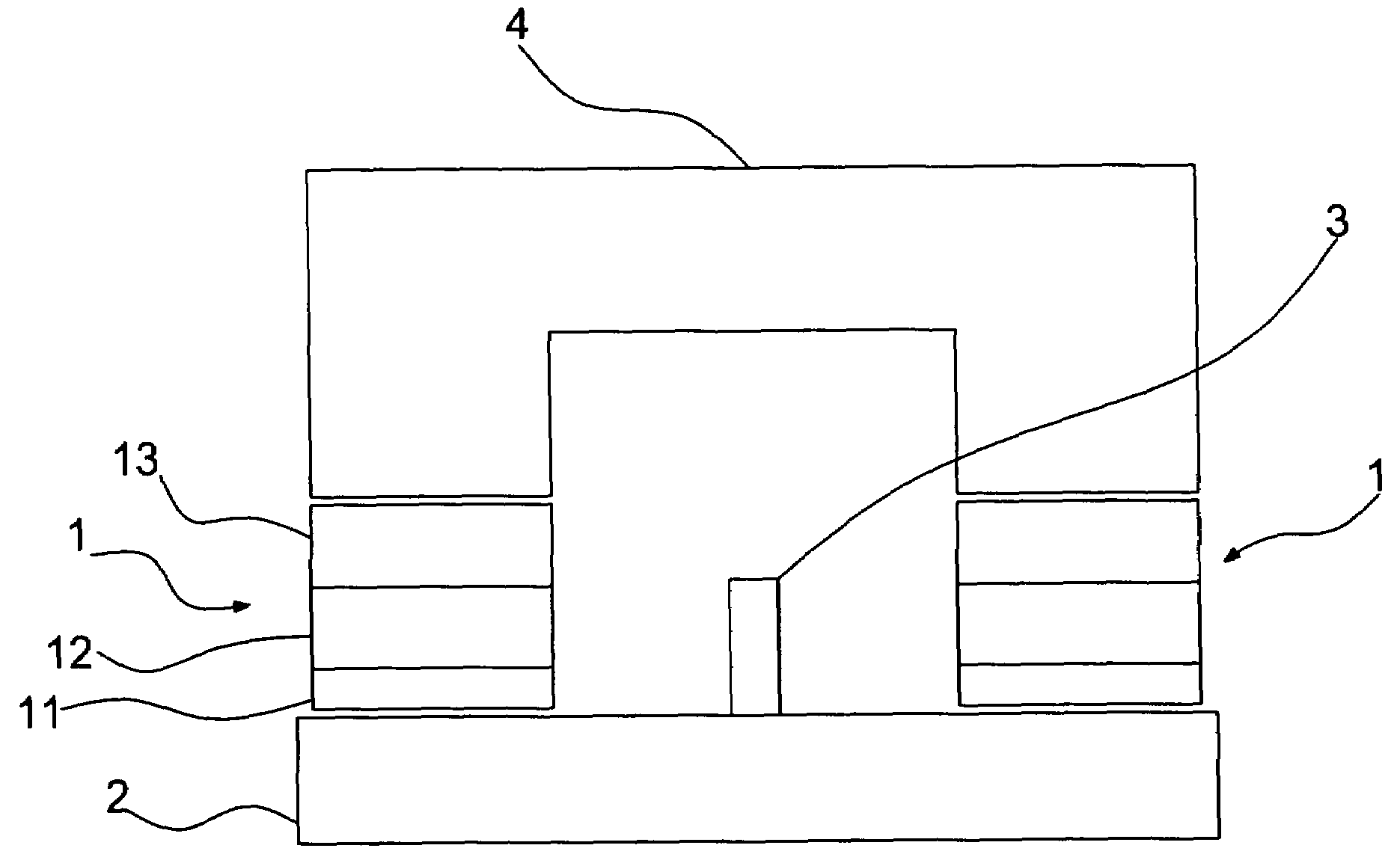
[0015]Please refer to FIG. 1, which is a view showing a structure of a preferred embodiment according to the present invention. As shown in the figure, the present invention is a copper-metalized compound diode device using an ohmic contact electrode, where the ohmic contact electrode 1 is composed of a palladium (Pd) layer 11, a germanium (Ge) layer 12 and a copper (Cu) layer 13; the layers (Pd / Ge / Cu) 11, 12, 13 are at first deposed on a compound semiconductor device 2; the compound semiconductor device 2 is a gallium arsenide (GaAs) device; then superfluous metal and photo resist are removed through a lift-off process; and, in the end, the layers 11, 12, 13 are processed through a rapid thermal annealing (RTA) to obtain the ohmic contact electrode. Therein, the ohmic contact electrode 1 obtains a low contact resistance through adjusting thi...


PUM

PropertyMeasurementUnit
thicknessaaaaaaaaaa
thicknessaaaaaaaaaa
thicknessaaaaaaaaaa

Abstract

The present invention provides an ohmic contact for a copper metallization whose heat diffusion is improved and cost is reduced. Therein, the ohmic contact is formed through a depositing and an annealing of three metal layers of Pd, Ge and Cu; and, the contact resistance of the ohmic contact is adjusted by the thicknesses of the three layers.

Description

FIELD OF THE INVENTION[0001]The present invention relates to a compound diode; more particularly, relates to obtaining an ohmic contact electrode having a low contact resistance by adjusting thicknesses of a palladium (Pd) layer, a germanium (Ge) layer and a copper (Cu) layer coordinated with an annealing process under a proper temperature, where the ohmic contact electrode is applied in a Cu metallization; and the contact resistance of a compound semiconductor device in the ohmic contact electrode is effectively improved and the cost is effectively reduced as well.DESCRIPTION OF THE RELATED ARTS[0002]Traditionally, the ohmic metals used by gallium arsenide (GaAs) devices are divided into two groups: one is a group of alloyed gold (Au) / germanium(Ge) / nickel(Ni); and the other is a group of Pd / Ge / Au through solid phase reactions. The group of Au / Ge / Ni is the most widely used ohmic contact now, which is obtained mainly through an eutectic reaction between Au and Ge and a diffusion of G...

Claims


Application Information

Patent Timeline
Patent Type & Authority Patents(United States)
IPC IPC(8): H01L23/48
CPCH01L21/28575
Inventor LEE, CHENG-SHIHCHANG, EDWARD YICHEN, KE-SHIAN
Owner NAT CHIAO TUNG UNIV
Features
  • R&D
  • Intellectual Property
  • Life Sciences
  • Materials
  • Tech Scout
  • Unparalleled Data Quality
  • Higher Quality Content
  • 60% Fewer Hallucinations
Learn More