Single substrate camera device with CMOS image sensor

a single-chip imaging and camera device technology, applied in the field of single-chip imaging sensors, can solve the problems of inordinate power dissipation and the control electronics have dissipated an inordinate percentage of the power of such imaging devices, and achieve the effects of compact image system, high fidelity and low loss

Inactive Publication Date: 2008-05-06
CALIFORNIA INST OF TECH
View PDF65 Cites 51 Cited by
  • Summary
  • Abstract
  • Description
  • Claims
  • Application Information

AI Technical Summary

Benefits of technology

[0006]Size minimization is also important. The development of the solid state charge coupled device (“CCD”) in the early 1970's led to more compact image systems. CCDs use a process of repeated lateral transfer of charge in an MOS electrode-based analog shift register. Photo-generated signal electrons are read after they are shifted into appropriate positions. However, the shifting process requires high fidelity and low loss. A specialized semiconductor fabrication process was used to obtain these characteristics.
[0011]Signal chain electronics that perform correlated double sampling (“CDS”) for noise reduction and amplification, and especially analog to digital converters (ADC), also dissipate significant power.

Problems solved by technology

However, the shifting process requires high fidelity and low loss.
CCDs are mostly capacitive devices and hence dissipate very little power.
The control electronics have dissipated an inordinate percentage of the power in such imaging devices.
Space-based imaging systems often have similar problems.
In addition, the need for various CCD clocking voltages (e.g. 7 or more different voltage levels) leads to numerous power supplies with their attendant inefficiencies in conversion.
Signal chain electronics that perform correlated double sampling (“CDS”) for noise reduction and amplification, and especially analog to digital converters (ADC), also dissipate significant power.
These inefficiencies included fill factor inefficiencies, fixed pattern noise, clock pick up, temporal noise and large pixel size.

Method used


Image

  • Single substrate camera device with CMOS image sensor
  • Single substrate camera device with CMOS image sensor
  • Single substrate camera device with CMOS image sensor

Examples


first embodiment

[0051]the present invention is a 128×128 CMOS photodiode type active pixel sensor that includes on chip timing, control and signal train electronics. A more detailed drawing of the chip is shown in FIG. 5. Asynchronous digital signals are converted by this chip to VS and VR analog outputs which are used to run the chip.

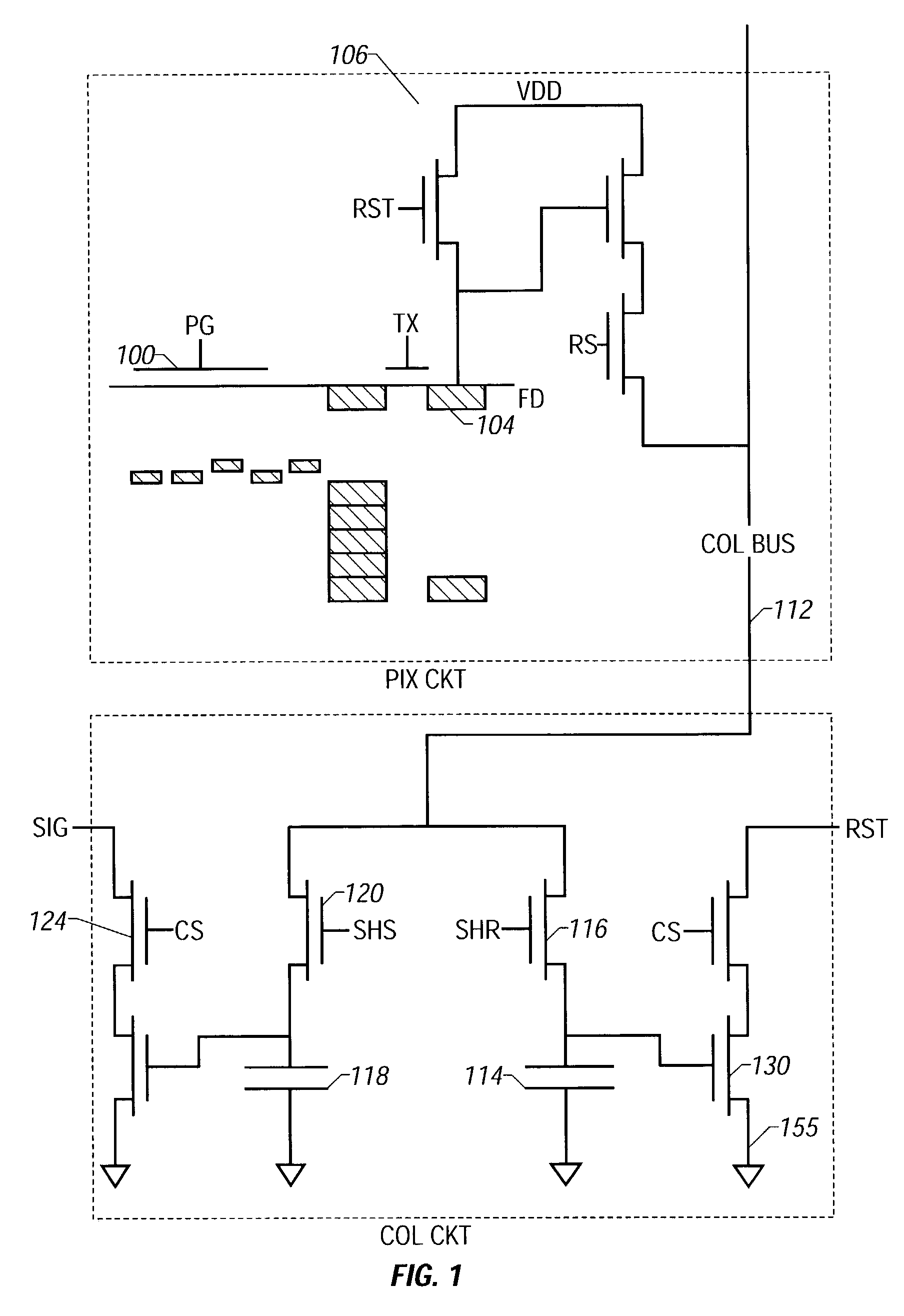
[0052]Pixel portion 500 includes a photodiode 502 which stores incident photons under photogate 504. The photons are integrated as electrons within the photogate well. The output is buffered by follower 508.

[0053]The rows are arranged into an array. A particular row is selected by the row transistor 514. This allows the information from within the selected pixel 500 to be passed to the column decoder circuitry. Reset transistor 530 is connected to a sink 532. Reset transistor is biased to a low potential level to allow all charge to bleed to sink 532, and hence hold the stored charge in reset. The system is removed from reset by biasing the gate to a level as shown. T...

second embodiment

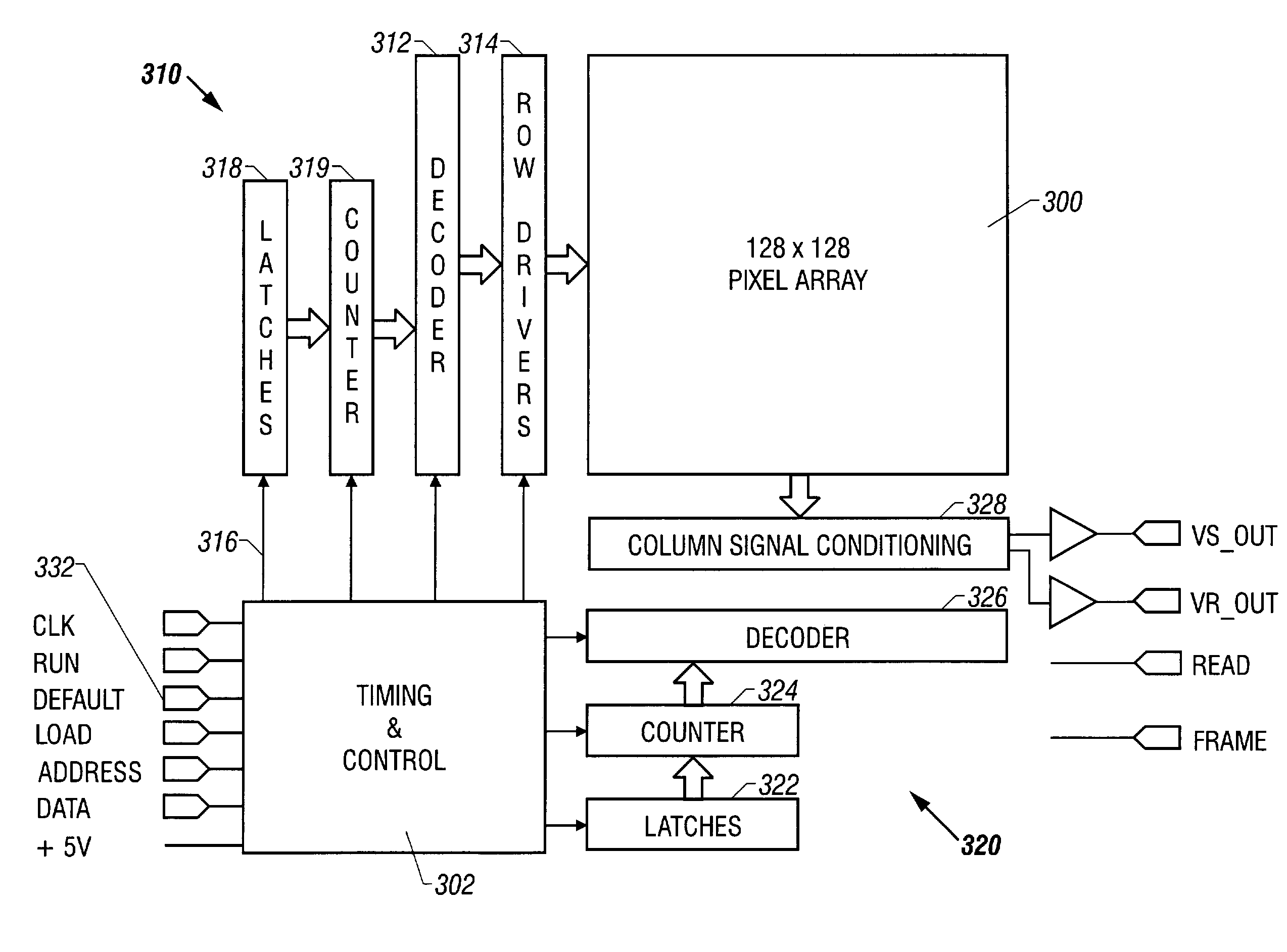
[0065]The second embodiment uses the block diagram of the chip architecture shown in FIG. 8. The analog outputs of VS_OUT (signal) and VR_OUT (reset), and digital outputs of FRAME and READ. The inputs to the chip are asynchronous digital signals. The chip includes addressing circuitry allowing readout of any area of interest within the 256×256 array. The decoder includes counters that are preset to start and stop at any value that has been loaded into the chip via the 8-bit data bus. An alternate loading command is provided using the DEFAULT input line. Activation of this line forces all counters to a readout window of 256×256.

[0066]A programmable integration time is set by adjusting the delay between the end of one frame and the beginning of the next. This parameter is set by loading a 32-bit latch via the input data bus. A 32-bit counter operates from one-fourth the clock input frequency and is preset at each frame from the latch. This counter allows forming very large integration...


PUM


Abstract

Single substrate device is formed to have an image acquisition device and a controller. The controller on the substrate controls the system operation.

Description

CROSS-REFERENCE TO RELATED APPLICATIONS[0001]This application is a divisional of U.S. application Ser. No. 09 / 120,856, filed Jul. 21, 1998, now U.S. Pat. No. 6,549,235; which is a continuation of U.S. application Ser. No. 08 / 789,608, filed Jan. 24, 1997, now U.S. Pat. No. 5,841,126; which claims the benefit of U.S. provisional application Ser. No. 60 / 010,678, filed Jan. 26, 1996 and is a continuation-in-part of U.S. application Ser. No. 08 / 558,521, filed Nov. 16, 1995; which is a continuation of U.S. application Ser. No. 08 / 188,032, filed Jan. 28, 1994, now U.S. Pat. No. 5,471,515. The disclosure of the prior applications is considered part of (and is incorporated by reference in) the disclosure of this application.ORIGIN[0002]The invention described herein was made in performance of work under NASA contract and is subject to the provisions of Public Law 96-517 (35 USC 202) in which the contractor has elected to retain title.FIELD OF THE INVENTION[0003]The present invention relates ...

Claims


Application Information

Patent Timeline
Patent Type & Authority Patents(United States)
IPC IPC(8): H04N5/335G11C19/28H01L27/146H01L27/148H01L31/0216H01L31/0232H04N5/345H04N5/353H04N5/357H04N5/361H04N5/363H04N5/365H04N5/369H04N5/374H04N5/3745H04N5/376H04N5/378H04N9/04
CPCG11C19/282G11C19/285H01L27/14601H01L27/14621H01L27/14627H01L27/14645H01L27/14656H01L27/14843H01L27/1485H01L27/14887H04N3/155H04N3/1562H04N3/1568H04N5/3575H04N5/361H04N5/363H04N5/3658H04N5/374H04N5/3745H04N5/37452H04N5/378H01L31/02162H01L31/0232H04N9/045H01L27/14603H04N25/616H04N25/65H04N25/677H04N25/63H04N25/771H04N25/70H04N25/77H04N23/10H04N25/76H04N25/75
Inventor FOSSUM, ERIC R.NIXON, ROBERT
Owner CALIFORNIA INST OF TECH
Why Eureka
Try Eureka