Method and system for measuring deep trenches in silicon

a technology of silicon trenches and trenches, applied in the field of silicon metrology, can solve the problems of the cost and delicateness of the components required by such systems, and reducing the practical utility of an ir spectroscopic ellipsometry system

Active Publication Date: 2008-05-06
KLA TENCOR TECH CORP
View PDF11 Cites 10 Cited by
  • Summary
  • Abstract
  • Description
  • Claims
  • Application Information

AI Technical Summary

Benefits of technology

[0013]Conventional IR spectroscopic ellipsometry systems provide a means for measuring the characteristics of trenches in silicon that would be difficult to otherwise determine. However, the IR handling components required by such systems are expensive and delicate, and can therefore reduce the practical utility of an IR spec

Problems solved by technology

However, the IR handling components required by such systems are expensive and delicate,

Method used


Image

  • Method and system for measuring deep trenches in silicon
  • Method and system for measuring deep trenches in silicon
  • Method and system for measuring deep trenches in silicon

Examples


Embodiment Construction

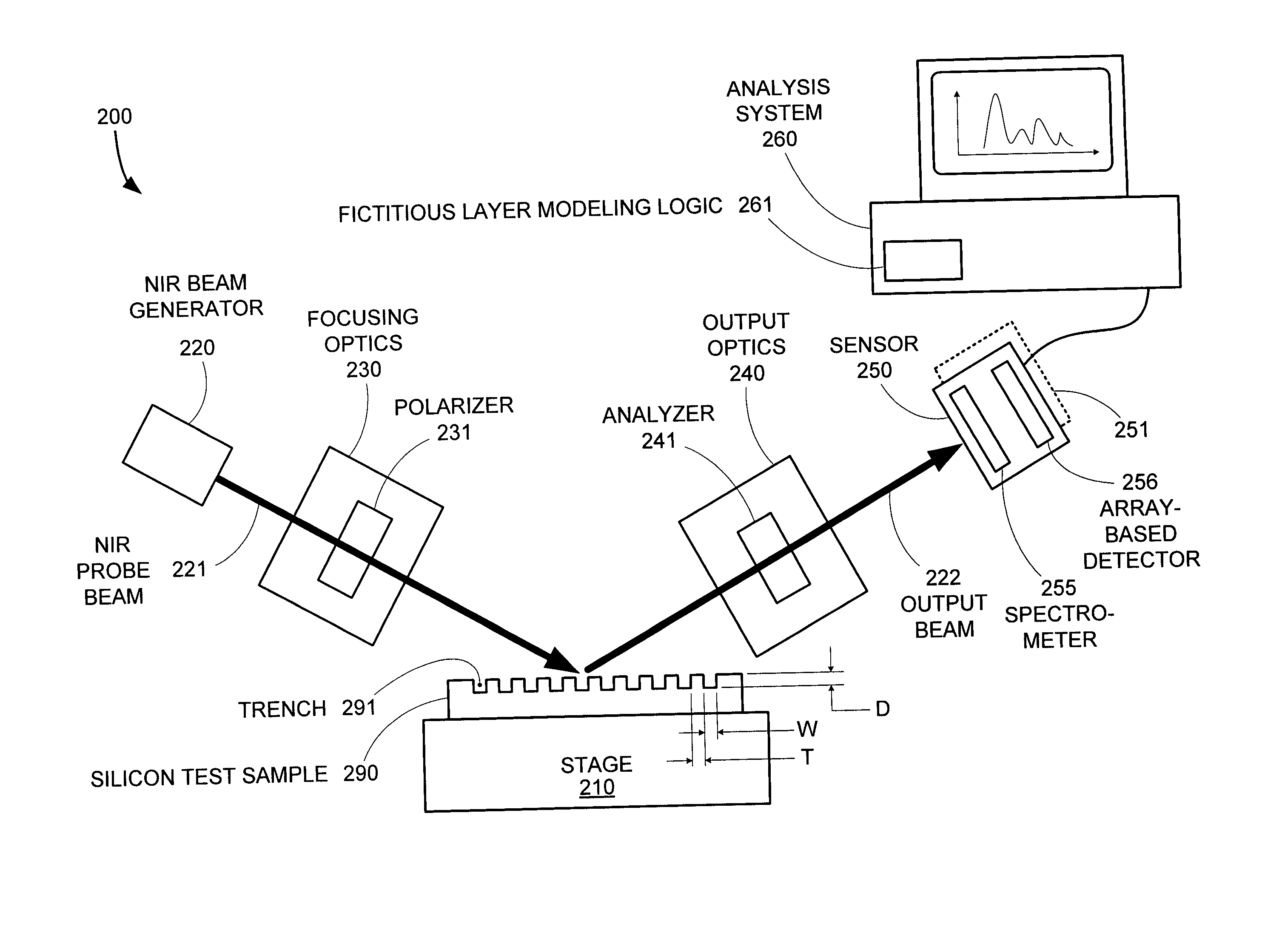
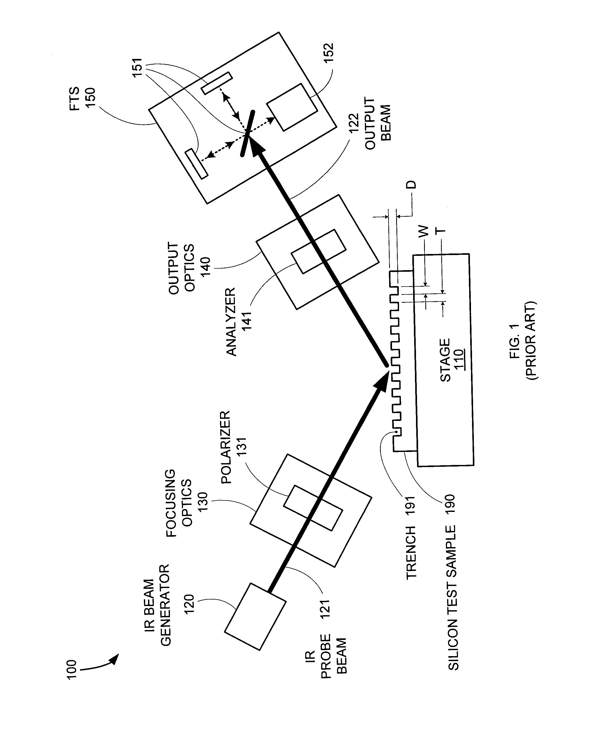
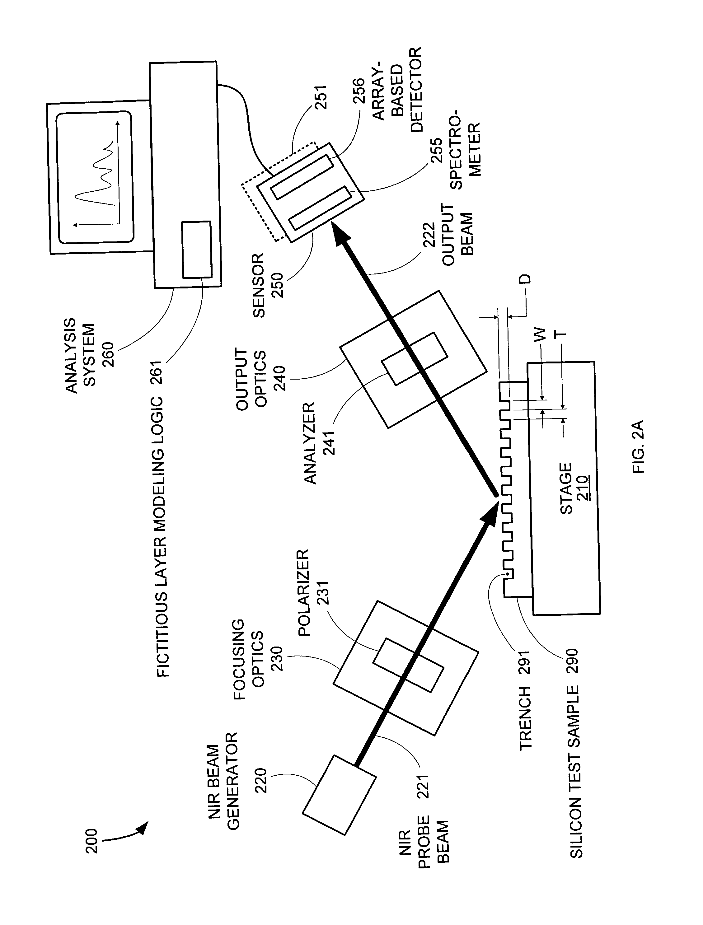
[0021]Conventional IR spectroscopic ellipsometry systems provide a means for measuring the characteristics of trenches in silicon that would be difficult to otherwise determine. However, the IR handling components required by such systems are expensive and delicate, and can therefore reduce the practical utility of an IR spectroscopic ellipsometry system. By performing spectroscopic ellipsometry using a probe beam in the near IR (NIR) range, the metrology capabilities of IR spectroscopic ellipsometry can be provided without the need for the costly and fragile IR-compatible components required by conventional IR spectroscopic ellipsometry systems.

[0022]FIG. 2A shows a NIR spectroscopic ellipsometry system 200 for analyzing a silicon test sample 290. NIR spectroscopic ellipsometry system 200 includes a stage 210, a NIR beam generator 220, focusing optics 230, output optics 240, a sensor 250, and an analysis system 260. Test sample 290, which is supported by stage 210, includes an arra...


PUM


Abstract

A spectroscopic ellipsometry system directs a near infra-red (NIR) probe beam at a test sample to allow metrology to be performed on vertical structures within the test sample. Because silicon is relatively transparent to NIR light, structural information can be determined from the polarization effects produced by the test sample, in a manner similar to that used with IR spectroscopic ellipsometry systems. However, unlike IR light, which requires delicate and costly optical and measurement components (e.g., vibration-sensitive Fourier transform sensors), NIR light can be directed and detected using more robust and inexpensive components (e.g., array-based detectors), thereby making a NIR spectroscopic ellipsometry system much more affordable and usable than conventional IR spectroscopic ellipsometry systems.

Description

BACKGROUND OF THE INVENTION[0001]1. Field of the Invention[0002]The invention relates to the field of semiconductor metrology, and in particular to a system and method for characterizing small trenches formed in silicon.[0003]2. Related Art[0004]Traditionally, semiconductor devices such as metal-oxide-semiconductor (MOS) transistors have been formed as essentially planar devices (sometimes referred to as “bulk” devices). Specifically, the gate dielectric and gate elements in such devices have been flat structures formed on the surface of a silicon wafer. However, in modern semiconductor devices, the need to achieve higher device performance in reduced die areas has led to the development of device designs that make greater use of the vertical dimension. For example, a “tri-gate” transistor can be formed by etching parallel trenches into a silicon wafer, thereby creating a “fin” of silicon between the trenches. A gate dielectric layer and a gate layer can then be formed that wrap ove...

Claims


Application Information

Patent Timeline
IPC IPC(8): G01J4/00
CPCG01B11/0641G01J4/04G01N21/211
Inventor JANIK, GARY R.FIELDEN, JOHN
Owner KLA TENCOR TECH CORP
Why Eureka
Try Eureka