Amorphous layers in a magnetic tunnel junction device

a tunnel junction and amorphous layer technology, applied in the field of magnetic tunnel junction devices, can solve the problem of high positive magnetostriction of cofeb, and achieve the effect of improving sensitivity

Inactive Publication Date: 2008-05-06
HEADWAY TECH INC +1
View PDF18 Cites 13 Cited by
  • Summary
  • Abstract
  • Description
  • Claims
  • Application Information

AI Technical Summary

Benefits of technology

[0010]It has been an object of at least one embodiment of the present invention to provide a TMR based device having improved sensitivity.
[0011]Another object of at least one embodiment of the present invention has been that said device have increased breakdown and reduced current characteristics.

Problems solved by technology

In practice, however, the extremely high positive magnetostriction of CoFeB is a source of problems such as a widely varying switching field distribution among MRAM arrays.

Method used


Image

  • Amorphous layers in a magnetic tunnel junction device
  • Amorphous layers in a magnetic tunnel junction device

Examples


Embodiment Construction

[0016]It is known that the smoothness of TMR films, especially, the dielectric layer, is critical to achieving high dr / r and other vital parameters such as breakdown voltage(Vbd), the dropping rate of TMR versus applying voltage, and V50 (voltage at which dR / R is reduced by 50%). Thus improved techniques are needed to obtain a smooth film prior to depositing the dielectric layer.

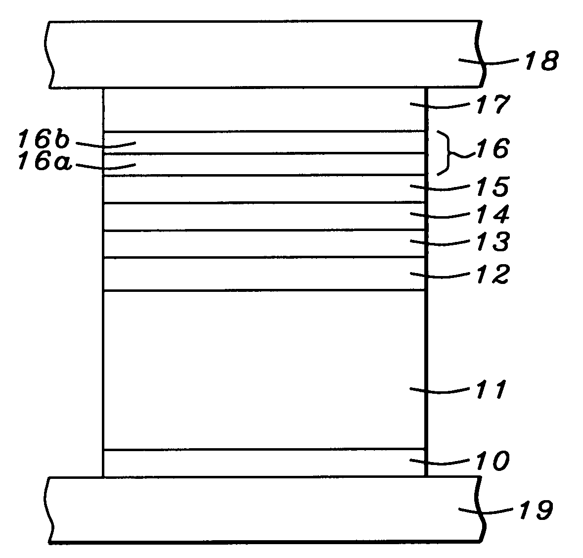
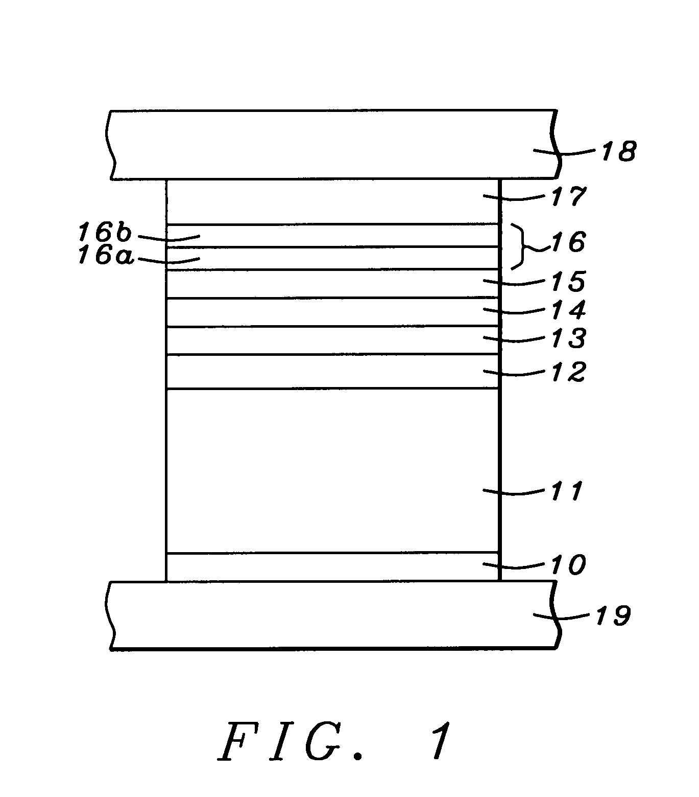
[0017]The structure of the invention is schematically illustrated in FIG. 1. Seen there are upper and lower conductive leads 18 and 19 with seed layer 10 being on layer 19. Antiferromagnetic layer 11 lies on seed layer 10 while AP2 and AP1 layers, 12 and 14 respectively, are immediately above it, with AFM decoupling layer 13 between them. Dielectric tunneling layer 15 lies on AP1 layer 14 and free layer 16 is on top of layer 15. Capping layer 17, on free layer 16, completes the structure.

[0018]To manufacture the invention, the layers are deposited in the order described in the previous paragraph and as shown...


PUM

PropertyMeasurementUnit
thicknessaaaaaaaaaa
conductiveaaaaaaaaaa
antiferromagneticaaaaaaaaaa

Abstract

An improved TMR device is disclosed. The ferromagnetic layers of the device, particularly those that contact the dielectric tunneling layer have an amorphous structure as well as a minimum thickness (of about 15 Å). A preferred material for contacting the dielectric layer is CoFeB. Ways of overcoming problems relating to magnetostriction are disclosed and a description of a process for manufacturing the device is included.

Description

FIELD OF THE INVENTION[0001]The invention relates to the design and fabrication of a magnetic tunnel junction (MTJ) Magnetic Random Access Memory (MRAM) array, and more specifically to magnetic tunnel junction devices with improved signal-to-noise ratio and switching behavior.BACKGROUND OF THE INVENTION[0002]The magnetic tunnel junction (MTJ) basically comprises two electrodes, which are layers of ferromagnetic material, separated by a tunnel barrier layer, which is a thin layer of insulating material. The tunnel barrier layer must be sufficiently thin so that there is a probability for charge carriers (typically electrons) to cross the layer by means of quantum mechanical tunneling. The tunneling probability is spin dependent, however, depending on the availability of tunneling states with different electron spin orientations. Thus, the overall tunneling current will depend on the number of spin-up vs. spin-down electrons, which in turn depends on the orientation of the electron sp...

Claims


Application Information

Patent Timeline
Patent Type & Authority Patents(United States)
IPC IPC(8): G11B5/39
CPCG11C11/15
Inventor GUO, YIMINMIN, TAIWANG, PO-KANG
Owner HEADWAY TECH INC
Why Eureka
Try Eureka