

Method of forming carbon-containing silicon nitride layer
a silicon nitride and carbon-containing technology, applied in the direction of coatings, transistors, chemical vapor deposition coatings, etc., can solve the problems of reducing the reliability and uniformity of the semiconductor device on the wafer, reducing the uniformity of the semiconductor device, and reducing the thickness of each layer and the process margin in each layer. achieve the effect of preventing boron diffusion, reducing the risk of forming a single layer, and improving the uniformity
- Summary
- Abstract
- Description
- Claims
- Application Information
AI Technical Summary
Benefits of technology
Problems solved by technology
Method used
Image

Examples
Embodiment Construction
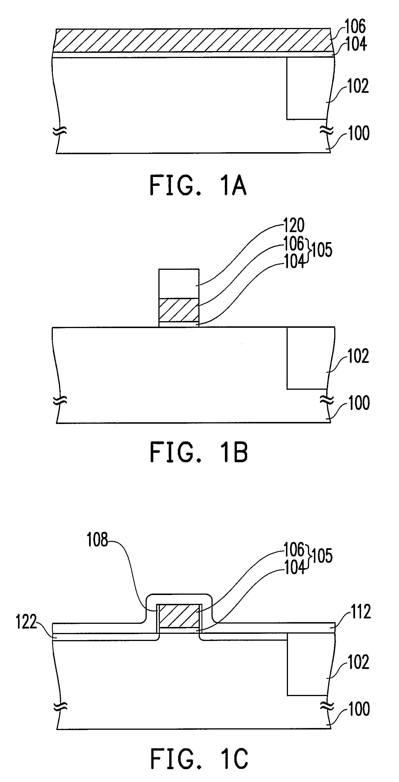
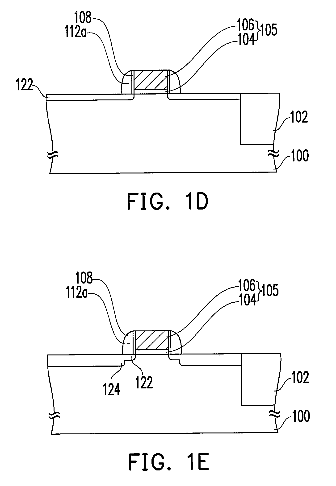
[0016]Reference will now be made in detail to the present preferred embodiments of the invention, examples of which are illustrated in the accompanying drawings. Wherever possible, the same reference numbers are used in the drawings and the description to refer to the same or like parts.
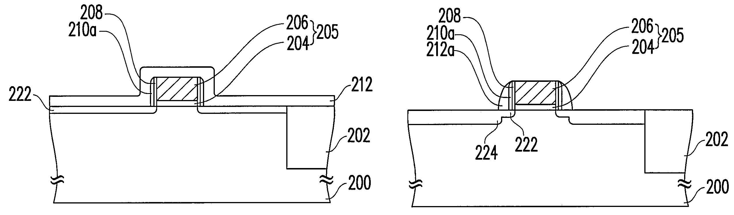
[0017]As mentioned above, as the line-width minimizes and the thickness of each layer shrinks, it is important to enhance the uniformity of certain layers, such as the silicon nitride layer for the offset spacer or the spacer for better-quality device or improved standardization of the devices within the wafer.
[0018]Currently, it is common to employ SiH4 and NH3 as the reactant gases for forming the silicon nitride layer by the single wafer tools. However, the obtained silicon nitride layer has inferior and unsatisfactory within wafer uniformity, wafer-to-wafer uniformity and lot-to-lot uniformity. Alternatively, furnace can be used to form the silicon nitride layer for the wafers in batch. However, ...
PUM
| Property | Measurement | Unit |
|---|---|---|
| pressure | aaaaa | aaaaa |
| reaction temperature | aaaaa | aaaaa |
| conductive | aaaaa | aaaaa |
Abstract
Description
Claims
Application Information