Delay locked loop in semiconductor memory device

a technology of semiconductor memory and delay loop, which is applied in the direction of generating/distributing signals, instruments, pulse techniques, etc., can solve the problems of large power consumption, large delay line block size, and inability to reduce the predetermined valu

Inactive Publication Date: 2008-05-20
INTELLECTUAL DISCOVERY CO LTD
View PDF6 Cites 24 Cited by
  • Summary
  • Abstract
  • Description
  • Claims
  • Application Information

AI Technical Summary

Benefits of technology

[0030]It is, therefore, an object of the present invention to provide a delayed lock loop (DLL), included in a semiconductor memory device, and its operating method for preventing a stuck fail in a dead-zone.
[0031]Also, it is another object of the present invention to provide a delayed lock loop, included in a semiconductor memory device, and its operating method for effectively reducing a delay value of a delay line block, e.g., the number of delay units included in the delay line block of the DLL.

Problems solved by technology

When an external clock signal of an external circuit is used in an internal circuit, a clock skew is generated from an internal circuit because of timing gap between the external clock signal and the internal clock signal.
However, in the initial operation state, it is impossible to reduce the predetermined value because the delayed feedback signal dfeedb passes through a minimum number of delay units.
Thus, for delaying the inputted signal by a desired delay value, each delay line block has too large size and consumes a large power.
Also, because, in the worse case, the DLL should delay the inputted signal by a most of one period of the reference clock signal, too much time for locking, i.e., synchronizing the inputted signal with the reference clock signal is needed.
However, above described DLL does not guarantee a stable operation when a phase difference between the external clock signal clk and the feedback signal fb is in a dead-zone.
Finally, the DLL shown in FIG. 3 still has a problem, i.e., cannot guarantee a stable operation when a phase difference is in the dead-zone.

Method used


Image

  • Delay locked loop in semiconductor memory device
  • Delay locked loop in semiconductor memory device
  • Delay locked loop in semiconductor memory device

Examples


first embodiment

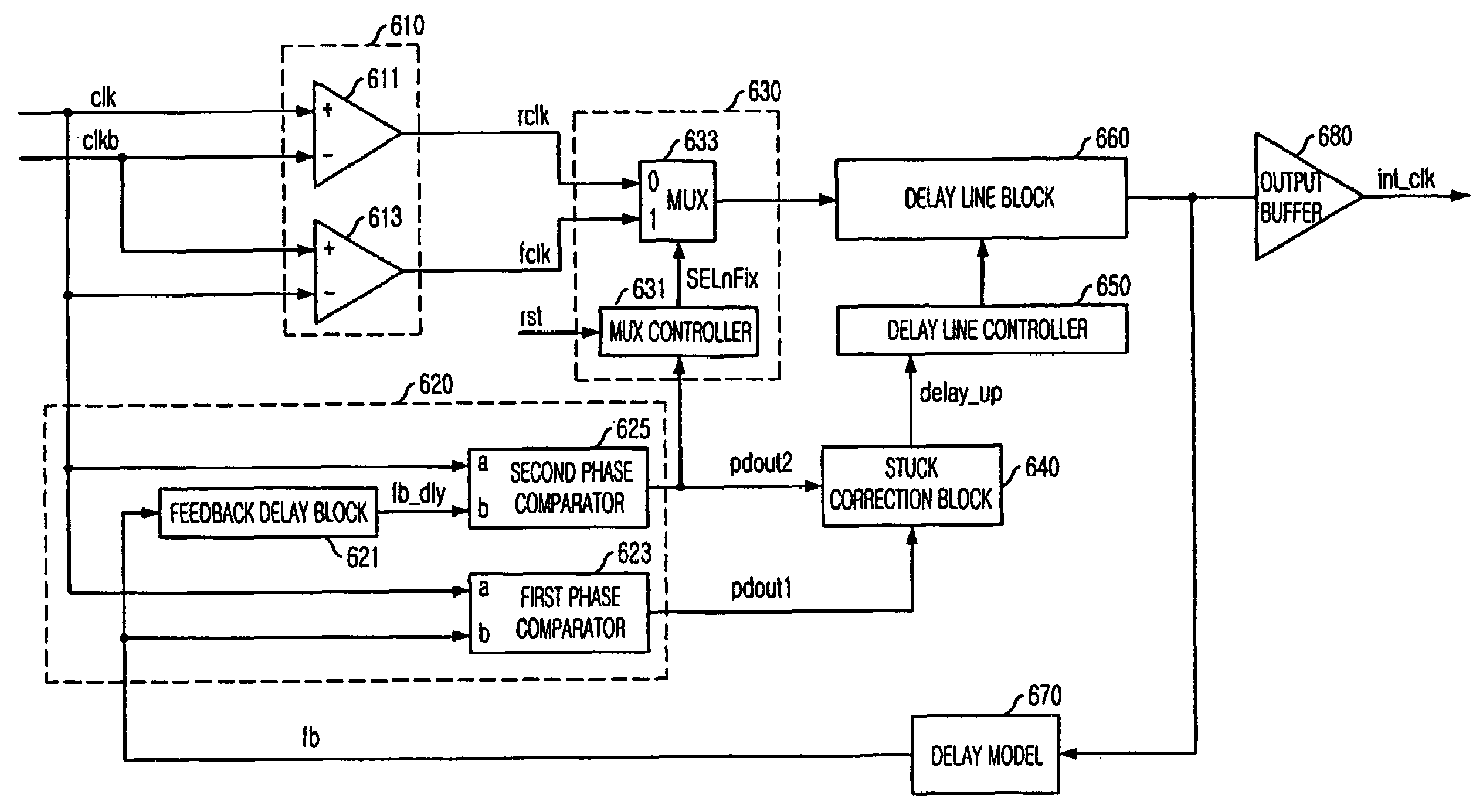
[0054]FIG. 6 is a block diagram depicting a DLL in accordance with the present invention.

[0055]As shown, the DLL includes a buffering block 610, a selecting block 630, a phase comparing block 620, a delay line block 660, a delay line control block 650, a stuck checking block 640, a delay modeling block 670 and an output buffer 680.

[0056]The clock buffering block 610 receives an external clock signal clk and a reverse external clock signal clkb to thereby generate a first and a second internal clock signals rclk and fclk. In detail, the clock buffering block 610 has a first clock buffer 611 and a second clock buffer 613. The first clock buffer 611 receives the external clock signal clk and the reverse external clock signal clkb and generating the first internal clock signal rclk which is corresponded to the external clock signal clk. Namely, the external clock signal clk is inputted through a non-inverting terminal; and the inverse external clock signal clkb is inputted through an in...

second embodiment

[0079]FIG. 12 is a block diagram depicting a DLL in accordance with the present invention.

[0080]As shown, the DLL is very similar to the DLL described in FIG. 6. Herein, differences between the DLLs in accordance with the first and second embodiments of the present invention are described.

[0081]Contrary to the phase comparing block 620, there is a selection and comparison block 1220. The selection and comparison block 1220 includes a second delay block 1221, a second multiplexer 1223 and a third phase comparator 1225.

[0082]In detail, the second delay block 1221 is same to the first delay block 621 shown in FIG. 6; and the third phase comparator 1225 is a kind of phase comparator shown in FIG. 9A. However, in the DLL in accordance with the second embodiment of the present invention, first of all, one of a delayed feedback signal fb_dly and a feedback signal fb is selected by the second multiplexer 1223 based on a currently clocking state signal lock_state outputted from a second stuc...


PUM


Abstract

A delayed lock loop for preventing a stuck fail in a dead-zone includes a clock buffering block for generating a first and a second internal clock signals; a phase comparison block for delaying a feedback signal by a first predetermined value and for respectively comparing a phase of a delayed feedback signal and a phase of the feedback signal with a phase of the external clock signal; a clock selecting block for selecting one of the first and second internal clock signals based on one comparison result to thereby generate a selected internal clock signal; a stuck checking block for determining a delay value based on the other comparison result; a delay line block for delaying the selected internal clock signal by the delay value; and an output buffer for buffering an outputted signal from the delay line block to thereby generating a DLL clock signal.

Description

FIELD OF INVENTION[0001]The present invention relates to a semiconductor memory device; and, more particularly, to a delay locked loop, included in the semiconductor memory device, for preventing a stuck fail in a dead-zone.DESCRIPTION OF PRIOR ART[0002]Generally, a clock signal of a system or a circuit is used as a reference for synchronizing an execution timing and guaranteeing an error-free high speed operation. When an external clock signal of an external circuit is used in an internal circuit, a clock skew is generated from an internal circuit because of timing gap between the external clock signal and the internal clock signal. A delay locked loop (hereinafter, referred as DLL) compensates the clock signal skew for equalizing a phase of the internal clock signal to that of the external clock signal.[0003]Moreover, the DLL is an apparatus for compensating the clock skew not only between the external clocks signal and the internal clock signal but also between the external clock...

Claims


Application Information

Patent Timeline
Patent Type & Authority Patents(United States)
IPC IPC(8): H03L7/06G06F1/10G11C7/00G11C8/00G11C11/407H03L7/081H04L7/033
CPCH03L7/0814H03L7/087G06F1/10G11C11/4076G11C7/1072G11C7/222G11C7/04H03L7/0816D03D47/34D03D47/277D03D49/02D03D51/02D03J1/24D03J2700/06
Inventor KWAK, JONG-TAE
Owner INTELLECTUAL DISCOVERY CO LTD
Why Eureka
Try Eureka