IC card

a technology of ic cards and e-cards, applied in the field of ic cards, can solve problems such as lowering printing properties, and achieve the effect of favorable printing properties and favorable flatness

Inactive Publication Date: 2008-05-27
SONY CORP
View PDF51 Cites 52 Cited by
  • Summary
  • Abstract
  • Description
  • Claims
  • Application Information

AI Technical Summary

Benefits of technology

[0022]Thus, by virtue of having a structure such that the sum A of the heights of the through holes or the heights B and C of the individual through holes fall within the above range, the surface of the card after being formed can secure favorable flatness to achieve favorable printing properties on the card surface.
[0023]In the IC card of the present invention, by adjusting

Problems solved by technology

As mentioned above, a conventional IC card cannot achieve satisfied flatness of the surface due to the uneven surface of the IC mounted portion of the IC module incorporated, and therefore the IC card having a rewritable display lay

Method used


Image

  • IC card
  • IC card
  • IC card

Examples


experimental example 1

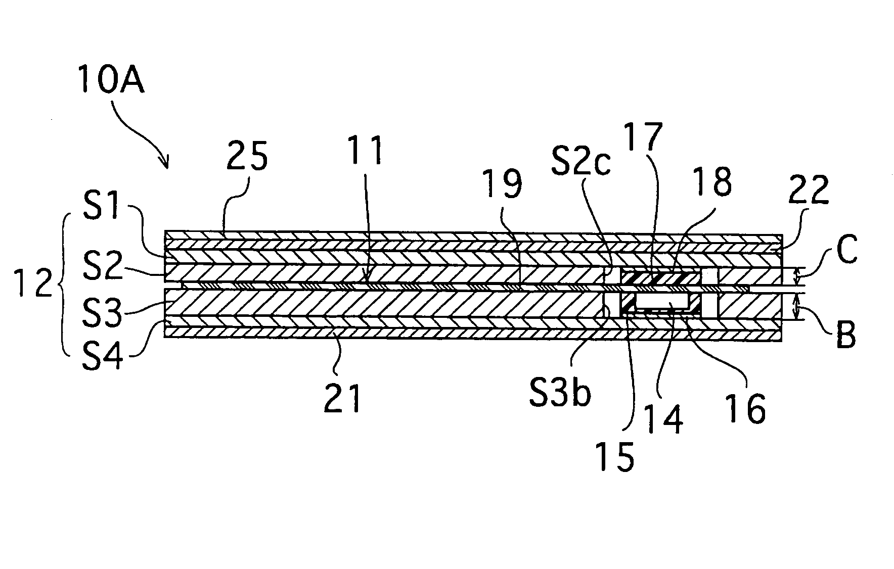
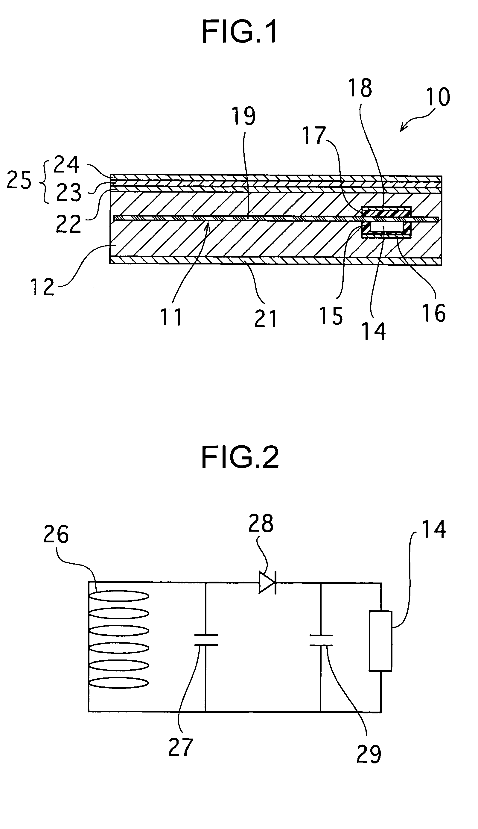
[0085]An IC card 10A having the structure example shown in FIG. 6 was prepared as a sample for evaluation.

[0086](1) First, an IC module 11 was produced as follows.

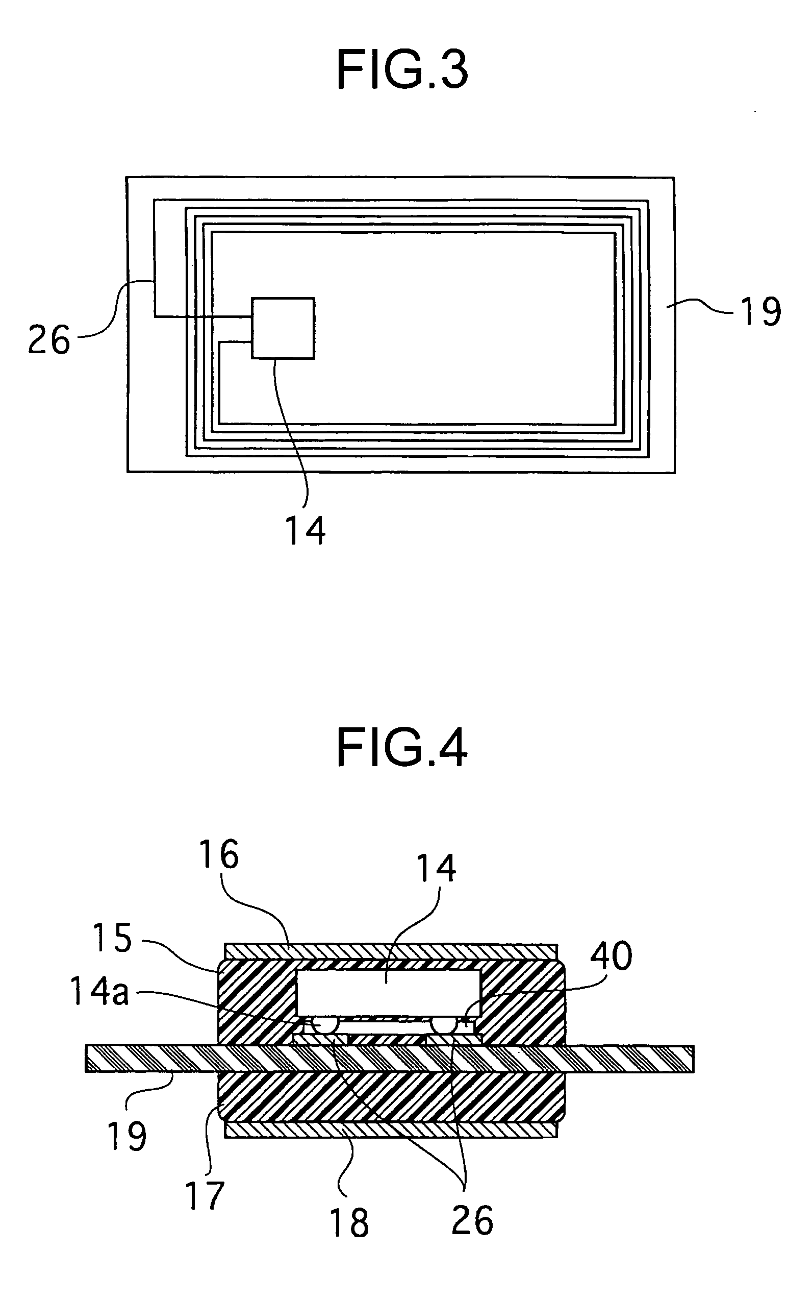
[0087]A polyester polyurethane resin solution was applied to an insulating substrate 19 comprised of polyethylene terephthalate having a thickness of 50 μm and dried to form a bonding layer having a thickness of 5 μm. Then, an aluminum foil was put on the adhesive layer and a resist was applied onto the aluminum foil, and then subjected to exposure and development treatment to form a resist pattern for antenna circuit, followed by etching treatment, thus forming an antenna pattern comprised of aluminum. The thickness of the insulating substrate 19 including the antenna pattern was 60 μm. Next, an IC chip (4 mm×4 mm) 14 was mounted by face down bonding on the IC mounted portion of the insulating substrate 19 through an anisotropic conductive layer 40 (see FIG. 4). Then, epoxy sealing resins 15, 17 are respectively applied t...

experimental examples 2 to 15

[0100]IC cards 10A having the structure example shown in FIG. 6 were individually prepared as samples for evaluation in accordance with substantially the same procedure as in Experimental Example 1 except that the inner core sheets S2, S3 having the respective thickness values shown in FIG. 91 were used in these Experimental Examples.

experimental example 16

[0101]An IC card 10A having the structure example shown in FIG. 6 was produced as a sample for evaluation in accordance with substantially the same procedure as in Experimental Example 1 except that, as constituent materials for the inner core sheets S2, S3, the materials shown in FIG. 9 were used in this Experimental Example.


PUM


Abstract

To provide an IC card, which secures satisfied flatness of the card surface to achieve good printing properties on the card surface. An IC card has a core layer which includes a plurality of sheet materials wherein inner core sheets adjacent to an IC module have through holes formed in a region corresponding to the IC mounted portion, wherein a relationship A=(B1+C1)±30 μm is satisfied, where A (μm) represents the sum of heights of the through holes, B1 represents a projection height on an IC mounted surface of the IC module, and C1 represents a projection height on an IC non-mounted surface. By virtue of having this structure, the IC card can secure card flatness sufficient to obtain satisfied printing properties with respect to the rewrite sheet.

Description

RELATED APPLICATION DATA[0001]The present application claims priority to Japanese Application(s) No(s). P2002-350640 filed Dec. 3, 2002, which application(s) is / are incorporated herein by reference to the extent permitted by law.BACKGROUND OF THE INVENTION[0002]1. Field of the Invention[0003]The present invention relates to an IC card having an information recording medium for use in, for example, an ID card (identification card), a membership card, a prepaid card, a cash card, a commuter's pass and the like. More particularly, the present invention is concerned with an IC card having both recorded information of electronic data and visible information.[0004]2. Description of Related Art[0005]Conventionally, in ID cards for identifying individuals, a method for magnetically or optically reading information recorded has been widely used in a credit card and the like. However, the techniques are popularized and the data in the cards is easily altered or forged cards are spread, and th...

Claims


Application Information

Patent Timeline
IPC IPC(8): G06K19/06G06K5/00G06Q40/00G07D11/00G07F19/00B42D15/10G06K19/07G06K19/077
CPCG06K19/077G06K19/07728G06K19/07749H01L2224/16H01L2924/01004H01L2924/01078H01L2924/07811H01L2924/01079H01L2924/01019H01L2924/00H01L2924/00014H01L2224/0401B42D25/22B42D25/305B42D25/45
Inventor OHTA, EIJIMATSUMURA, SHINICHI
Owner SONY CORP
Why Eureka
Try Eureka