Page-buffer and non-volatile semiconductor memory including page buffer

a non-volatile semiconductor and memory technology, applied in static storage, digital storage, instruments, etc., can solve the problems of signal distortion and data errors, reduced layout area of the various circuits, and disadvantages of the non-volatile memory device described abov

Active Publication Date: 2008-05-27
SAMSUNG ELECTRONICS CO LTD
View PDF13 Cites 37 Cited by
  • Summary
  • Abstract
  • Description
  • Claims
  • Application Information

AI Technical Summary

Problems solved by technology

Conventional non-volatile memory devices described above suffer from a number of drawbacks, particularly as the layout area of the various circuits is reduced as the memory devices become more integrated to meet demands for higher memory capacities.
The resultant coupling noise between adjacent internal data lines IDB can cause signal distortion and data errors.
In some cases, this can result in the data being flipped.
Further, the heavy output load of the internal data lines IDB makes it necessary to increase the output drive capability of the page buffers, which can be problematic when space and power resources are limited.
This relatively large number of lines must be attended by a large layout area for the bus region of the device, thus occupying scarce space resources.

Method used


Image

  • Page-buffer and non-volatile semiconductor memory including page buffer
  • Page-buffer and non-volatile semiconductor memory including page buffer
  • Page-buffer and non-volatile semiconductor memory including page buffer

Examples


Embodiment Construction

[0060]The present invention will now be described by way of preferred but non-limiting embodiments.

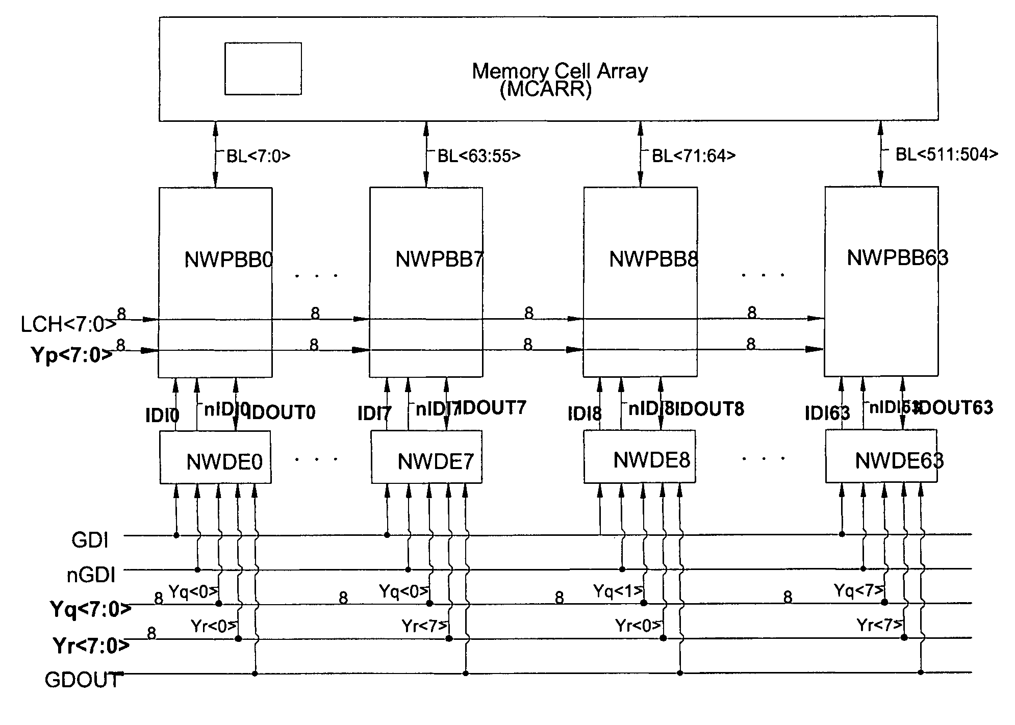
[0061]FIG. 11 is a schematic block diagram of a nonvolatile semiconductor memory device according to an embodiment of the present invention.

[0062]Referring to FIG. 11, the nonvolatile semiconductor memory device of this example includes a memory cell array MCARR, page buffer blocks NWPBB63:0>, first and second global input lines GDI and nGDI, a global output line GDOUT, y address signal lines Yp7:0>, Yq7:0> and Yr7:0>, read latch signal lines LCH7:0>, and page buffer decoders NWDE63:0>.

[0063]The memory cell array MCARR includes a matrix array of memory cells, word lines WL (not shown in FIG. 11) and bit lines BL511:0>. In the example of this embodiment, the memory cells are flash memory cell transistors.

[0064]Internal input lines IDI63:0> and nIDI63:0>, and internal output lines IDOUT63:0>, are connected between the page buffer decoders NWDE63:0> and corresponding page buffer blocks NW...


PUM


Abstract

In one aspect, a non-volatile memory device is provided which is operable in a programming mode and a read mode. The memory device includes a memory cell array which includes a plurality of non-volatile memory cells, a plurality of word lines, and a plurality of bit lines. The memory device further includes an internal data output line for outputting data read from the bit lines of the memory array, and a page buffer operatively connected between a bit line of the memory cell array and the internal data output line. The page buffer includes a sense node which is selectively connected to the bit line, a latch circuit having a latch node which is selectively connected to the sense node, a latch input path which sets a logic voltage of the latch node in the programming mode and the read mode, and a latch output path which is separate from the latch input path and which sets as logic voltage of the internal date output line according to the logic voltage of the latch node.

Description

BACKGROUND OF THE INVENTION[0001]1. Field of the Invention[0002]The present invention generally relates to semiconductor memory devices, and more particularly, the present invention relates to page buffer circuits and other circuits utilized in non-volatile semiconductor memory devices.[0003]2. Description of the Related Art[0004]The demand for electrically programmable and electrically erasable nonvolatile memory devices has increased dramatically in recent years. Such devices are at least partially characterized by the ability to maintain stored data even in the absence of supplied power. The use of so-called flash memories has become especially popular, particularly, but not exclusively, in the context of portable devices such as digital cameras, cell phones, personal data assistants (PDAs), and laptop computers. Flash memories, such as NAND-type flash memories, are capable of storing large amounts of data in a relatively small area.[0005]As background discussion, the basic opera...

Claims


Application Information

Patent Timeline
Patent Type & Authority Patents(United States)
IPC IPC(8): G11C11/34
CPCG11C16/0483G11C16/26G11C16/08G11C16/24
Inventor LEE, SUNG-SOOLIM, YOUNG-HOCHO, HYUN-CHULCHAE, DONG-HYUK
Owner SAMSUNG ELECTRONICS CO LTD
Why Eureka
Try Eureka