Quantifying and predicting the impact of line edge roughness on device reliability and performance

a technology of reliability and performance, which is applied in the field of semiconductor/solid-state device testing/measurement, instruments, adaptive control, etc., can solve the problems of ler appearing in fabricated structures, unsatisfactory structural defects in the dielectric layer, and ler may occur, so as to reduce or eliminate the manufacture of defective or unreliable devices. , the effect of reducing the cost of manufacturing

Inactive Publication Date: 2008-05-27
GLOBALFOUNDRIES INC
View PDF13 Cites 9 Cited by
  • Summary
  • Abstract
  • Description
  • Claims
  • Application Information

AI Technical Summary

Benefits of technology

[0013]An advantage of the present invention is simplification and reduction in the cost of manufacturing by providing real-time feedback information to the fabrication facility regarding the impact structural defects may have on device reliability and performance. In this way, structural defects that adversely affect device reliability may be detected and corrected on a real-time basis which will reduce or eliminate the manufacture of defective or unreliable devices.
[0014]Another advantage of the present invention is that accuracy and precision of wafers is improved by employing the various testing and prediction procedures. The present invention also improves reliability and efficiency of both the fabrication process and devices fabricated via in line production testing and information communication with the fabrication facility. The signal to noise ratio of the devices may also be greatly improved according to an aspect of the present invention.

Problems solved by technology

During semiconductor fabrication, undesirable structural defects in the dielectric layers, such as line edge roughness (LER) may occur.
In addition, LER appearing in fabricated structures can occur as a result of damage to the patterned photoresist during an etch process.
LER present in the metal lines of the device could negatively impact the BEOL reliability of the device through various factors.
First, the effective spacing of the metal lines may be reduced, resulting in an increase in the electrical field for a given voltage difference between the lines.

Method used


Image

  • Quantifying and predicting the impact of line edge roughness on device reliability and performance
  • Quantifying and predicting the impact of line edge roughness on device reliability and performance
  • Quantifying and predicting the impact of line edge roughness on device reliability and performance

Examples


Embodiment Construction

[0029]The present invention will now be described with reference to the drawings, wherein like reference numerals are used to refer to like elements throughout. The present invention will be described with reference to systems and methods for utilizing wafer level electrical test results in order to facilitate predicting the reliability of wafers in a wafer fabrication environment. It should be understood that the description of these exemplary aspects are merely illustrative and that they should not be taken in a limiting sense.

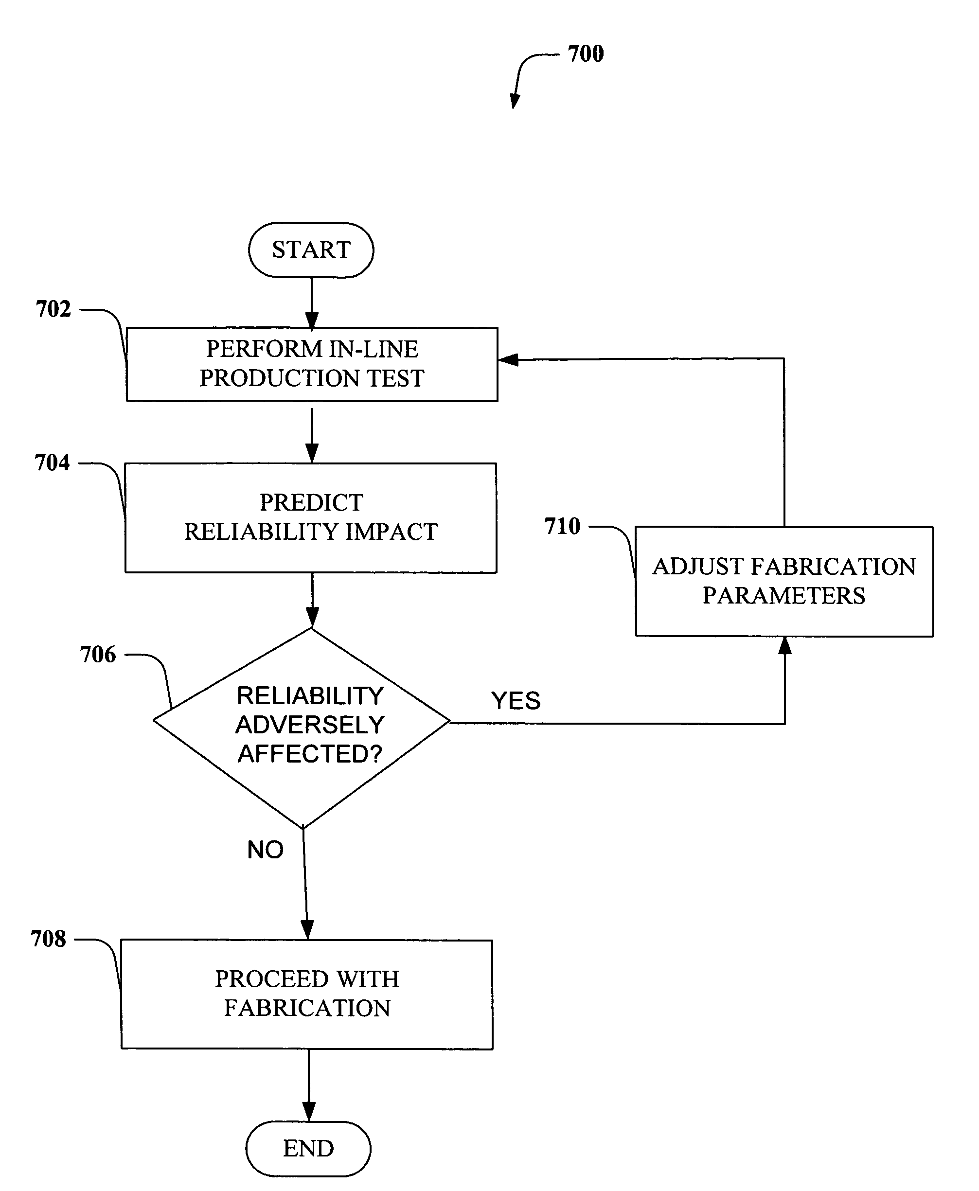
[0030]Certain methodologies that can be implemented in accordance with the present invention are illustrated. While, for purposes of simplicity of explanation, the methodologies are shown and described as a series of blocks, it is to be understood and appreciated that the present invention is not limited by the order of the blocks, as some blocks can, in accordance with the present invention, occur in different orders and / or concurrently with other blocks fr...


PUM


Abstract

Systems and methods are disclosed for testing semiconductors at the wafer level, specifically, systems and methods are disclosed that quantify line-edge roughness in terms of electrical properties and the impact of the line-edge roughness on device reliability and performance. A voltage ramp dielectric breakdown (VRDB) test is used to measure the breakdown voltage of the inter-digitated fingers of a semiconductor device. The distribution of breakdown voltage is used to measure the median breakdown voltage and the outliers which fan the extrinsic tail. Thereby, VRDB is used to quantify the impact LER will have on device reliability and performance. The systems and methods also provide a feedback tool to the fabrication process to control line edge roughness to a desired specification.

Description

FIELD OF INVENTION[0001]The present invention relates generally to semiconductor fabrication, and more particularly to systems and methodologies to facilitate predicting, during the wafer manufacturing process, the impact of line edge roughness on device reliability and performance.BACKGROUND OF THE INVENTION[0002]There has been an increasing demand for semiconductor devices with higher packing densities that are smaller and more precisely formed. Achieving these objectives continues to drive the semiconductor manufacturing industry to improve every aspect of the fabrication process. While there are numerous steps involved with fabricating semiconductors, the steps can be broken down into two major processes. The first major process is the front end of line (FEOL) process which begins with a starting wafer up to the first-metal cut. The second major process is the back end of line (BEOL) process which has been defined as all process steps after the first-metal cut.[0003]Due to high-...

Claims


Application Information

Patent Timeline
Patent Type & Authority Patents(United States)
IPC IPC(8): G06F15/18G05B13/00
CPCH01L22/20
Inventor MARATHE, AMIT P.GABRIEL, CALVIN T.
Owner GLOBALFOUNDRIES INC
Why Eureka
Try Eureka