Phase-change TaN resistor based triple-state/multi-state read only memory

a phase-change tan resistor and read-only memory technology, applied in semiconductor devices, digital storage, instruments, etc., can solve problems such as data loss, achieve the effects of increasing the information density of the memory, reducing the complexity of the feol, and increasing the density of the on-chip memory

Active Publication Date: 2008-06-03
INT BUSINESS MASCH CORP
View PDF21 Cites 17 Cited by
  • Summary
  • Abstract
  • Description
  • Claims
  • Application Information

AI Technical Summary

Benefits of technology

[0007]The present invention provides a nonvolatile memory such as, for example, a ROM or EPROM, in which the information density of the memory is increased relative to a conventional nonvolatile memory that includes only two logic state devices. Specifically, the present invention provides a simple two-terminal element as a base for a ROM. In accordance with the present invention, the device element of the present invention is built at the back-end-of-the-line (BEOL) instead of the front-end-of-the-line (FEOL), which could significantly minimize the increasing FEOL complexity and increase on-chip memory density by stacking them together within different BEOL levels without consuming extra die surface area. The device element of the present invention also offers multilevel storage and low-voltage operation, which offer another advantage to increase density and reduce power. By adopting the inventive device element, a fast, simple, high-density, one-time programmable nonvolatile memory is provided.
[0010]The physics of such resistance change is attributed to phase transition inside TaN. A relevant property of such a phase change is the ability of TaN to keep information for very long times. By increasing input electrical power even more (over a threshold), a drastic resistance drop can be observed. The resistance drop described above is attributed to a second amorphous phase transition inside TaN. Therefore, the TaN based element (i.e., thin film resistor stack) can be optimally coupled with a non-linear Si-containing device (such as a diode which can be part of a field effect transistor) to form an electrically alterable one-time EPROM array with short access time, low-cost, high-density, and low power operation.

Problems solved by technology

In volatile memory, the data stored is lost when the power of the device is tuned off.

Method used


Image

  • Phase-change TaN resistor based triple-state/multi-state read only memory
  • Phase-change TaN resistor based triple-state/multi-state read only memory
  • Phase-change TaN resistor based triple-state/multi-state read only memory

Examples


Embodiment Construction

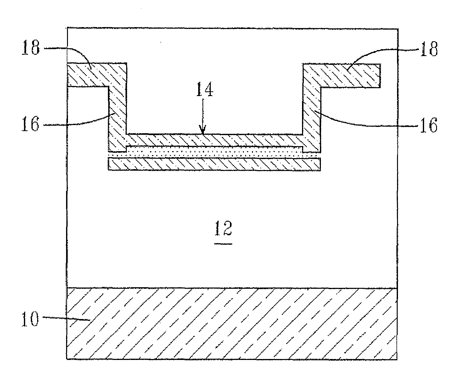
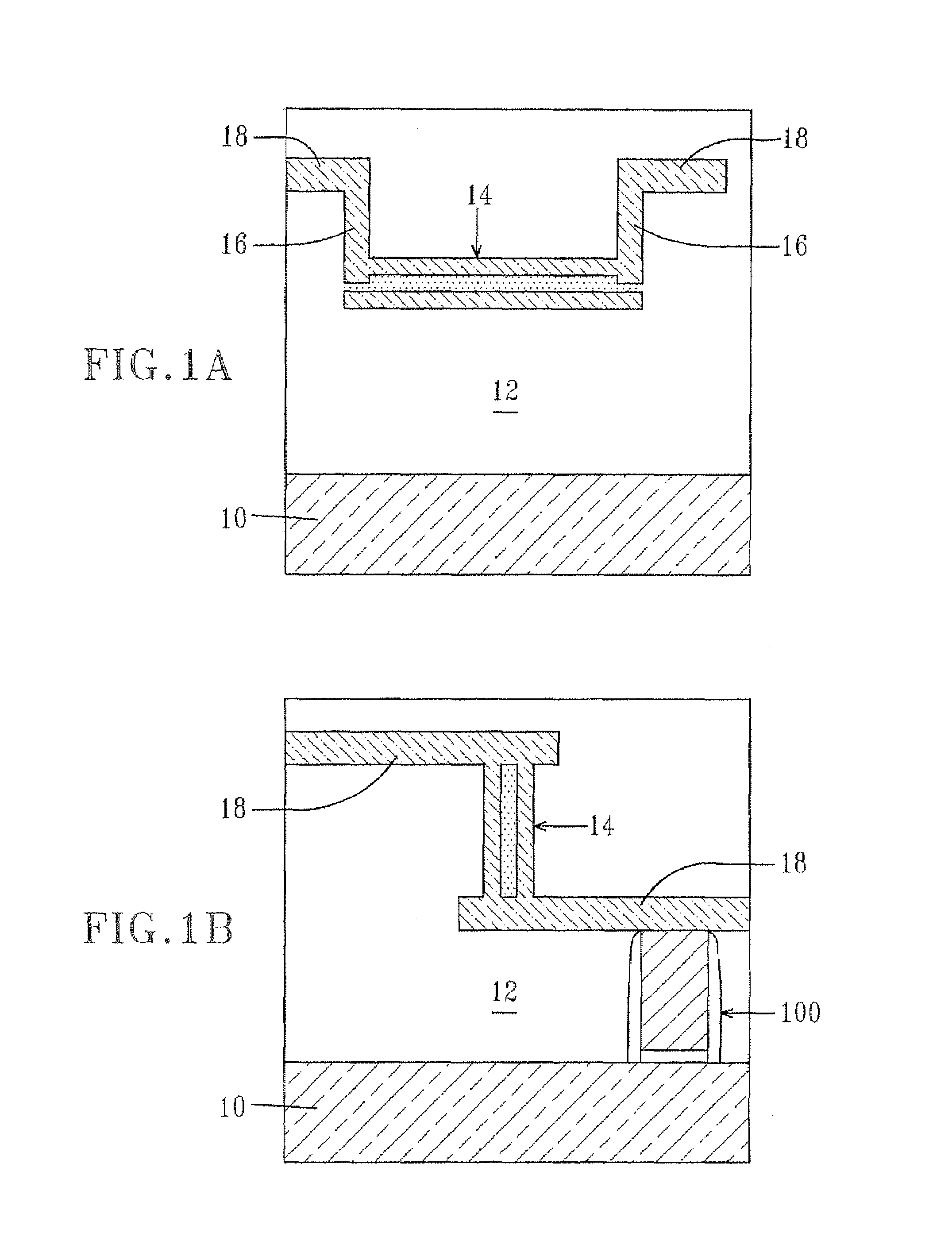
[0041]The present invention, which provides a three or more logic state nonvolatile IC memory cell including a phase-change TaN resistor, will now be described in greater detail by referring to the following discussion as well as drawings that accompany the present application. As stated above, the present invention provides a two-terminal element as a base for one-time electrically programmable read-only memory (OEPROM's). The device element is built at the BEOL (i.e., during interconnect formation within at least one of the interlevel dielectrics of the interconnect structure) instead of the FEOL, which could significantly minimize the increasing FEOL complexity and increase on-chip memory density by stacking them together within different BEOL levels without increasing die surface area. This simple device also offers multilevel storage and low-voltage operation, which offers another advantage to increase density and reduce power. By adopting the inventive device, a fast, simple, ...


PUM


Abstract

The present invention relates to a nonvolatile memory such as, for example a ROM or an EPROM, in which the information density of the memory is increased relative to a conventional nonvolatile memory that includes two logic state devices. Specifically, the nonvolatile memory of the present invention includes a SiN / TaN / SiN thin film resistor embedded within a material having a thermal conductivity of about 1 W / m-K or less; and a non-linear Si-containing device coupled to the resistor. Read and write circuits and operations are also provided in the present application.

Description

FIELD OF THE INVENTION[0001]The present invention relates to a semiconductor integrated circuit (IC), and more particularly, to an IC memory cell and chip including at least a thin film phase-change resistor coupled to a non-linear Si-containing semiconductor device. In accordance with the present invention, the impedance of the phase-change resistor may be modulated by varying an applied voltage, which causes joule heating induced phase change in one of the resistor elements. The variation in impedance may be correlated to a plurality of device states or memory values. An IC memory chip contains thousands, even millions of memory cells, but all of them may share one write circuit and one read circuit.BACKGROUND OF THE INVENTION[0002]A nonvolatile memory is a solid-state device that does not need to have its memory contents periodically refreshed. Nonvolatile type memory devices are used in various applications in which logic instructions must be stored for later recall, including, ...

Claims


Application Information

Patent Timeline
Patent Type & Authority Patents(United States)
IPC IPC(8): H01L29/02H01L47/00
CPCG11C11/56G11C11/5678G11C11/5692G11C13/0004G11C17/16G11C17/18H01L45/145H01L45/1233H01L45/06H01L45/1226H01L27/101H01L27/2409H10B63/20H10N70/823H10N70/231H10N70/883H10N70/826
Inventor AITKEN, JOHN M.CHEN, FENFENG, KAI D.
Owner INT BUSINESS MASCH CORP
Why Eureka
Try Eureka