
Reference buffer using current mirrors and source followers to generate reference voltages

a reference buffer and source follower technology, applied in the field of reference buffers, can solve the problems of degrading the performance of pipelined adc, affecting the performance of reference buffers, and vrefp, vrefn, vcom typically suffer from dynamic kickback, so as to achieve fast speed, control the bandwidth and output impedance of reference buffers, and wide bandwidth

Active Publication Date: 2008-06-03
DIALOG SEMICONDUCTOR INC
View PDF10 Cites 12 Cited by
  • Summary
  • Abstract
  • Description
  • Claims
  • Application Information

AI Technical Summary

Benefits of technology

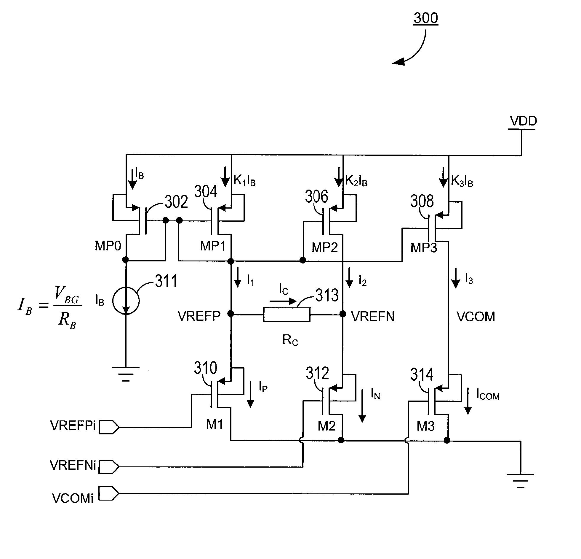
The present invention provides a reference buffer that can generate multiple reference voltages using a single circuit. The buffer includes a first current mirror, a second current mirror, and a third current mirror, which are driven by a first, second, and third transistor, respectively. A first source follower and a second source follower receive the first and second reference voltages, respectively. A first resistor is connected between a first node and a second node, and a second resistor is connected between a second node and a third node. The voltage difference between the first reference voltage and the second reference voltage is maintained as the voltage difference between the second reference voltage and the second initial reference voltage. The size of the transistors is adjusted to force the voltage difference between the first reference voltage and the second reference voltage to be equal to the voltage difference between the second reference voltage and the second initial reference voltage. The reference buffer has a wide bandwidth and no external capacitor is needed to stabilize the nodes of the output reference voltages. The bandwidth and output impedance of the reference buffer can be controlled by adjusting the sizes of the MOSFETs forming the current mirror to meet fast speed, high resolution requirements.

Problems solved by technology

These reference voltages VREFP, VREFN, and VCOM typically suffer from dynamic kickback from the MDACs and need to settle within the required accuracy for a given number of bits for an ADC within half of the sampling clock period.
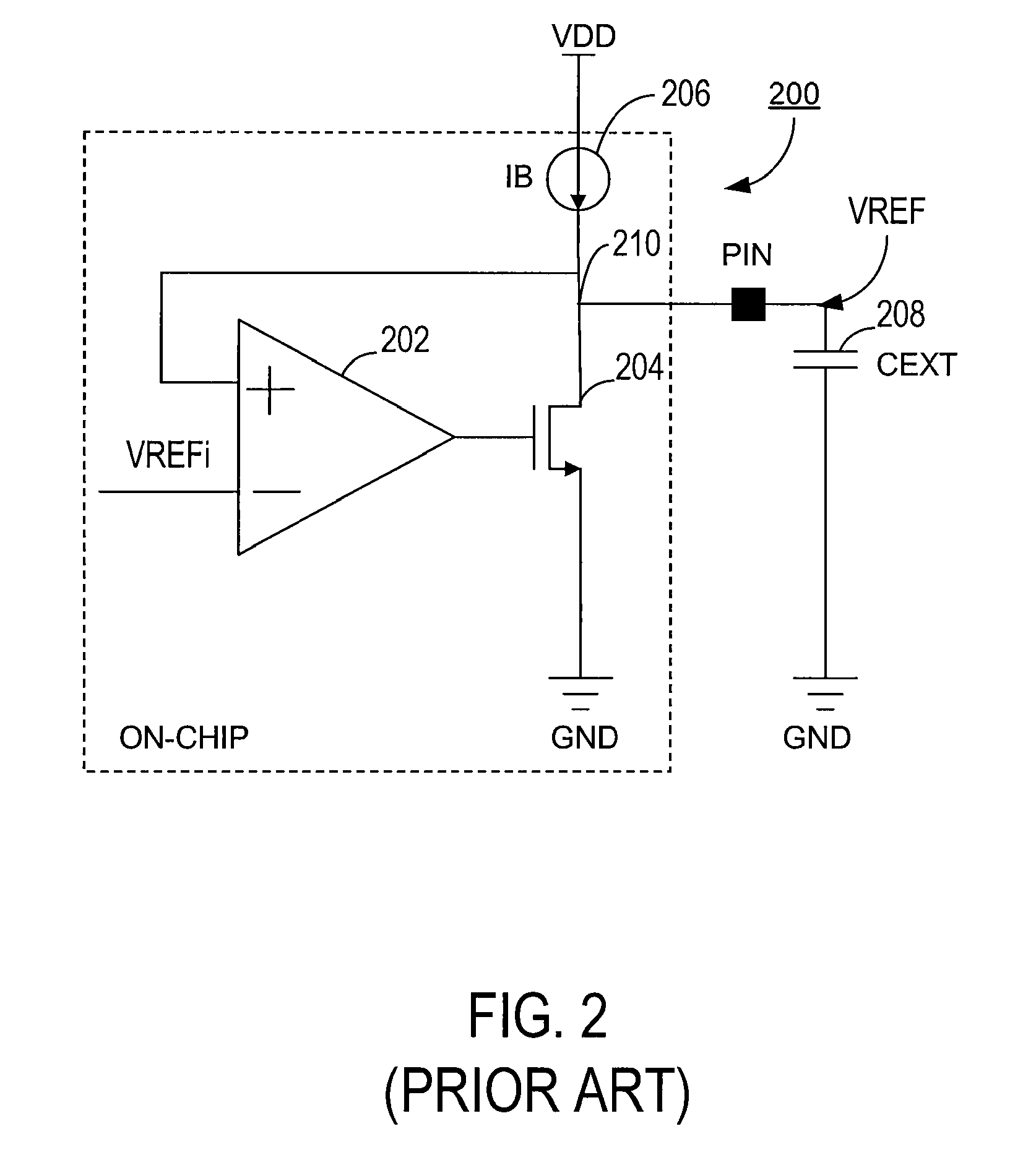
However, adding this external capacitor 208 adds significant cost to the reference buffer 200, and the parasitic inductance caused by the IC pin dedicated to the external capacitor 208 degrades the performance of the pipelined ADC.

Method used


Image

  • Reference buffer using current mirrors and source followers to generate reference voltages
  • Reference buffer using current mirrors and source followers to generate reference voltages
  • Reference buffer using current mirrors and source followers to generate reference voltages

Examples


Embodiment Construction

[0028]The Figures (FIG.) and the following description relate to preferred embodiments of the present invention by way of illustration only. It should be noted that from the following discussion, alternative embodiments of the structures and methods disclosed herein will be readily recognized as viable alternatives that may be employed without departing from the principles of the claimed invention.

[0029]Reference will now be made in detail to several embodiments of the present invention(s), examples of which are illustrated in the accompanying figures. It is noted that wherever practicable similar or like reference numbers may be used in the figures and may indicate similar or like functionality. The figures depict embodiments of the present invention for purposes of illustration only. One skilled in the art will readily recognize from the following description that alternative embodiments of the structures and methods illustrated herein may be employed without departing from the pr...


PUM


Abstract

A reference buffer includes a first current mirror, a second current mirror, a first source follower coupled in series to a branch of the first current mirror and receiving a first initial reference voltage and outputting a first reference voltage, a second source follower coupled in series to a branch of the second current mirror and receiving a second initial reference voltage and outputting a second reference voltage, and a resistor coupled between a first node and a second node outputting the first and second reference voltages, respectively. The first node is disposed between the first current mirror and the first source follower and the second node is disposed between the second current mirror and the second source follower. The voltage difference between the first reference voltage and the first initial reference voltage is substantially same as that between the second reference voltage and the second initial reference voltage.

Description

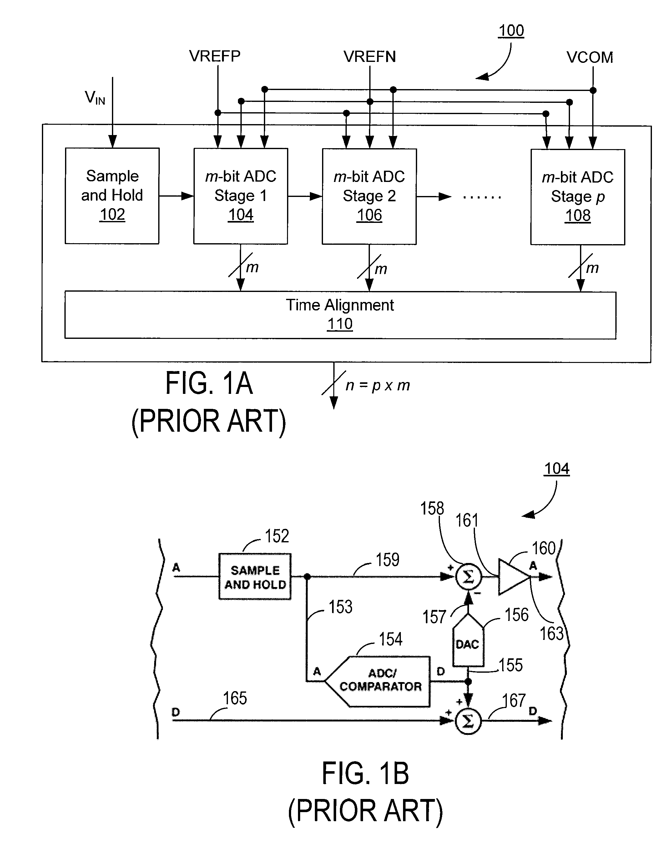
BACKGROUND OF THE INVENTION[0001]1. Field of the Invention[0002]The present invention relates to a reference buffer and, more specifically, to an on-chip CMOS reference buffer generating reference voltages for use in a pipelined analog to digital converter.[0003]2. Description of the Related Art[0004]Pipelined analog to digital converters (ADC) are widely used in a variety of electronic devices. A pipelined analog to digital converter divides the analog-to-digital conversion task into several consecutive stages. FIG. 1A is a simplified block diagram illustrating a conventional pipelined ADC 100, and FIG. 1B is a simplified block diagram illustrating one of the m-bit analog-to-digital conversion stages of the pipelined ADC 100. The pipelined ADC 100 includes a sample and hold circuit 102, and a plurality (p) of m-bit analog-to-digital conversion (ADC) stages 104, 106, . . . , 108. The sample-and hold circuit 102 holds the analog input voltage (VIN) while the ADC stages 104, 106, . . ...

Claims


Application Information

Patent Timeline
Patent Type & Authority Patents(United States)
IPC IPC(8): H03M1/38
CPCG05F3/262H03M1/168
Inventor LIANG, ENZHUJIN, XUECHENG
Owner DIALOG SEMICONDUCTOR INC
Learn More