

V-coupled-cavity semiconductor laser
a semiconductor laser and cavity-coupled cavity technology, applied in lasers, laser construction details, transmission, etc., can solve the problems of reducing the fabrication yield, reducing the complexity of such lasers, and increasing the cost, so as to achieve optimal single-mode selectivity of lasers
- Summary
- Abstract
- Description
- Claims
- Application Information
AI Technical Summary
Benefits of technology
Problems solved by technology
Method used
Image

Examples
Embodiment Construction
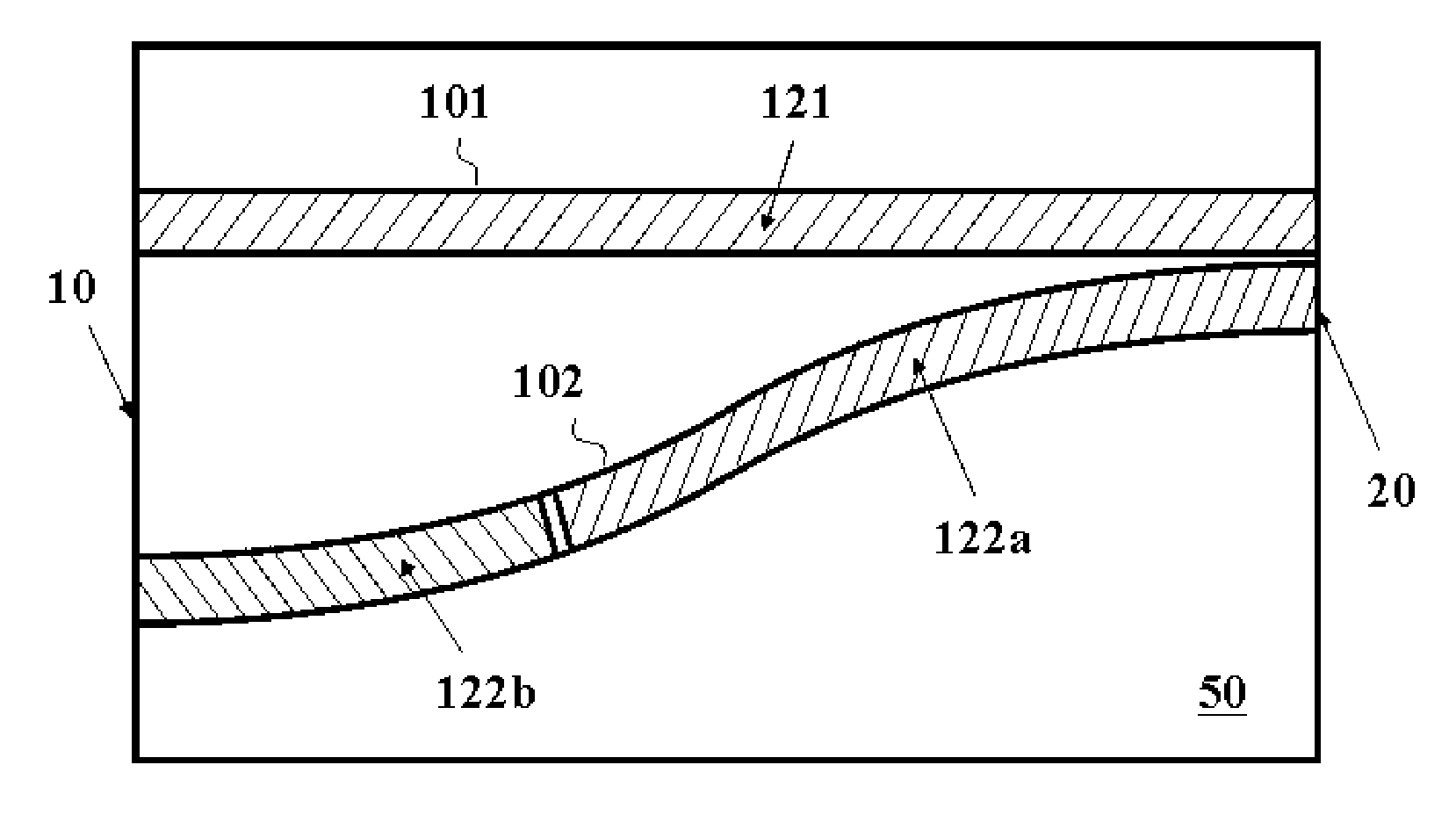
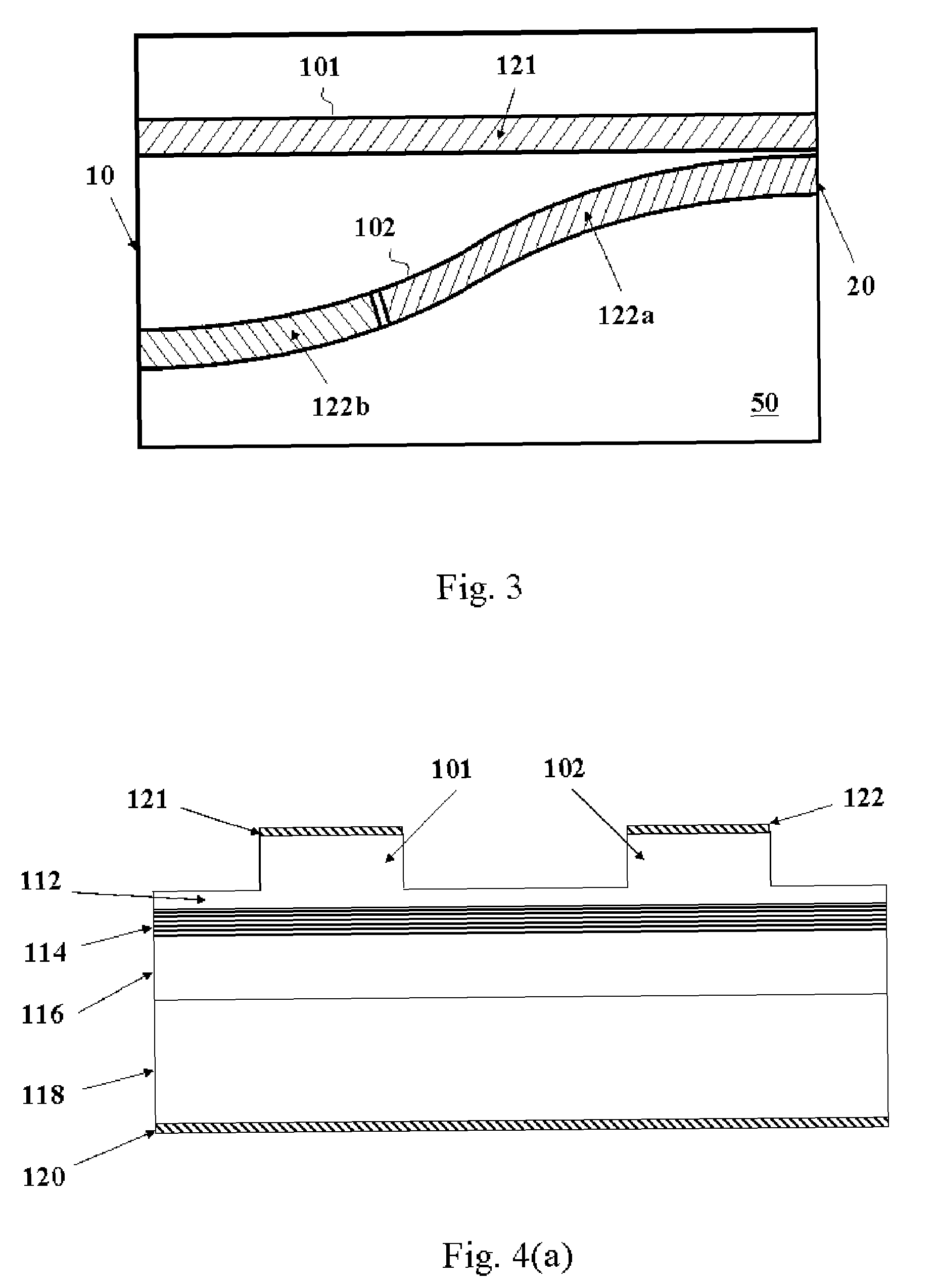
[0036]FIG. 3 shows the top view of a monolithic wavelength switchable V-coupled-cavity laser in accordance with one embodiment of the present invention. The laser consists of two waveguides branches 101 and 102 forming a substantially V-shaped geometry, disposed on a semiconductor chip 50. They are closely spaced or touching on one end (i.e. the closed end) but far apart on the other end (i.e. the open end). Bounded by cleaved facets 10 and 20 (or etched trenches in an alternative embodiment), each of the two waveguide branches forms a Fabry-Perot cavity. Near the end facet 20 where the two waveguides are closely spaced or touching, a small amount of light is coupled from one cavity to the other, due to evanescent coupling or overlap of mode fields. An electrode 121 is deposited on top of the waveguide branches 101 while two electrodes 122a and 122b are deposited on top of the waveguide branches 102. In operation, the electrodes 121a and 122a are injected with essentially fixed curr...
PUM
 Abstract
Description
Claims
Application Information