True color flat panel display module

a flat panel display and modular technology, applied in the field of true color flat panel modular electronic displays, can solve the problems of lack of brightness, failure of flat panel displays incorporating leds to reach their theoretical potential in the actual marketplace, lack of brightness, etc., and achieve the effect of increasing the overall thickness required for the display

Inactive Publication Date: 2008-06-10
CREE INC
View PDF119 Cites 19 Cited by
  • Summary
  • Abstract
  • Description
  • Claims
  • Application Information

AI Technical Summary

Benefits of technology

[0019]Accordingly, it is an object of the present invention to provide a flat panel display that can produce a full range of true colors and that can do so in module form so that large panel displays can be formed of such modules and yet without increasing the overall thickness required for the display.
[0024]In a further aspect, the invention comprises a full-range, true color flat panel display module comprising a pixel matrix formed of n rows and 2n columns, where n is a power of 2; and means for driving the matrix in two sets of blocks with n / 2 rows per block, to thereby allow more brightness per pixel, lower clock update speeds, and a generally more efficient use of power.

Problems solved by technology

To date, however, flat panel displays incorporating LEDs have failed to reach their theoretical potential in the actual marketplace.
LED flat panel displays have lacked success in penetrating the technology and the marketplace for several reasons.
Because the human eye is less responsive at 700 nm, the devices tend to lack brightness and thus are often limited to applications where maximum brightness is less critical.
Similarly, silicon carbide blue devices have only been commercially available for approximately a decade.
Such materials are generally limited to silicon carbide, gallium nitride, certain other Group III nitrides, and diamond.
For a number of reasons, all of these materials have been historically difficult to work with, generally because of their physical properties, their crystallography, and the difficulty in forming them into both bulk crystals and epitaxial layers, both of which are generally (although not exclusively) structural requirements for light emitting diodes.
The net effect is that SiC LEDs are limited in brightness.
Thus, although their recent availability represents a technological and commercial breakthrough, their limited brightness likewise limits some of their applicability to displays, particularly larger displays that are most desirably used in bright conditions; e.g.. outdoor displays used in daylight.
Group III nitrides present their own set of problems and challenges.
As another disadvantage, flat panel displays in the current art are generally only “flat” in comparison to CRTs, and in reality have some substantial thickness.

Method used


Image

  • True color flat panel display module
  • True color flat panel display module
  • True color flat panel display module

Examples


Embodiment Construction

[0038]The present invention is a thin flat panel display module that can produce a full range of-true colors. As set forth above, the term true color refers to a much greater range of colors than have been previously available from prior devices incorporating either light emitting diode or other technologies.

[0039]The invention provides a thin flat panel display module suitable as a subassembly for construction of any size, although predominantly wall sized, thin flat panel displays.

[0040]The modules of the invention are capable of displaying portions of any visual image, either moving or stationary, in either any color or combination of colors. By combining modules horizontally and vertically, virtually any size of display board can be constructed.

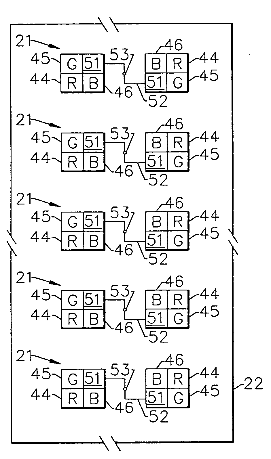
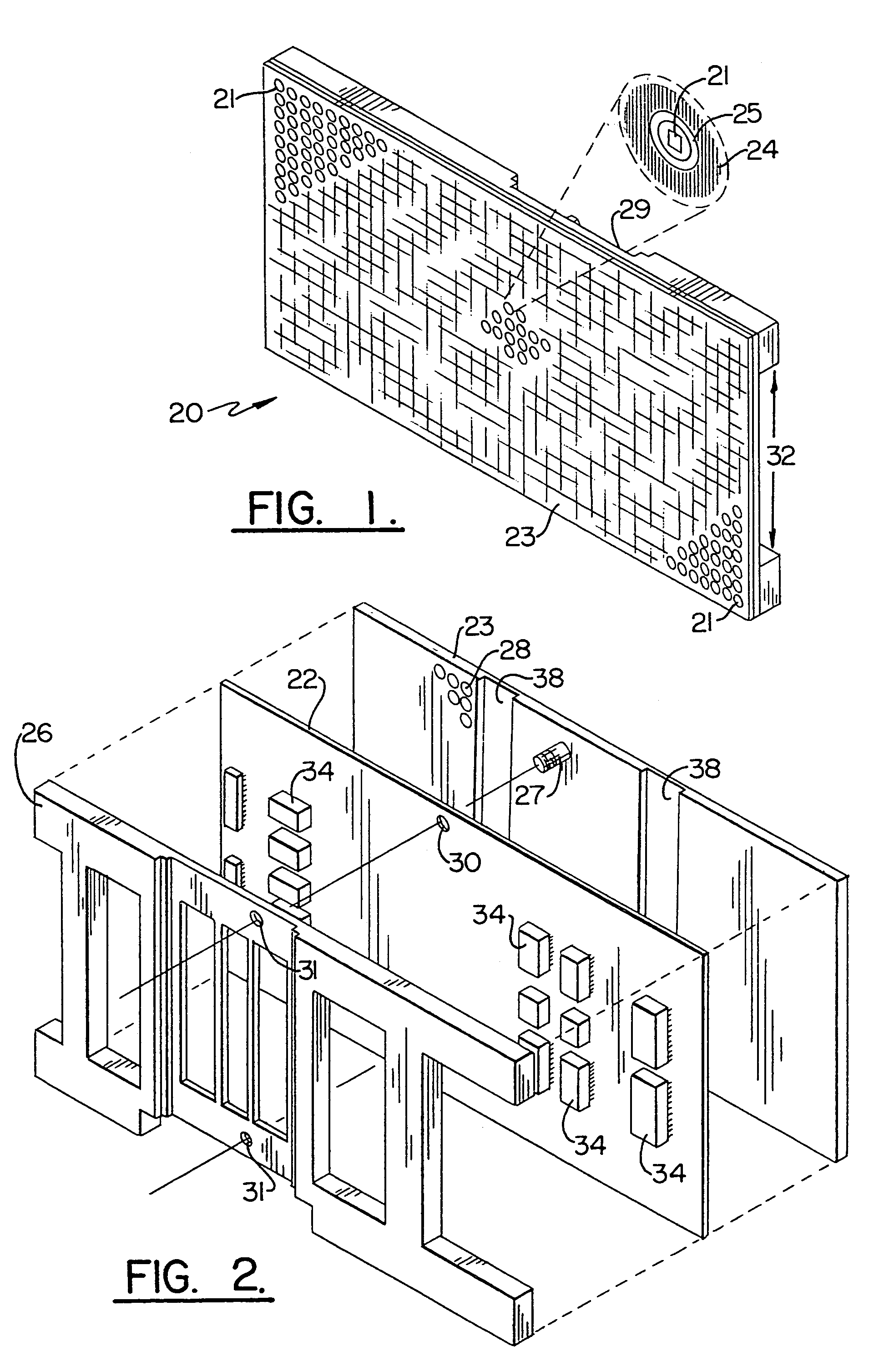
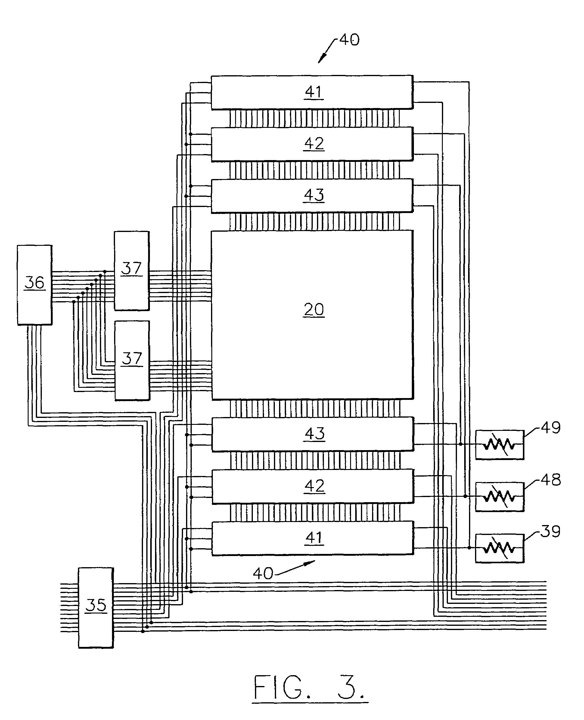
[0041]FIGS. 1 and 2 are front and rear perspective views showing the module broadly designated at 20. A matrix of substantially flat full color pixels, several of which are labelled as 21 in FIG. 1 are mounted on a first surface of a prin...


PUM


Abstract

A full color flat panel display module is formed of a matrix of pixels in rows and columns. Each pixel is formed of respective red, green and blue solid state light emitting diodes that can form any color on that portion of a CIE curve that falls within a triangle whose sides are formed by a line on the CIE curve between 430 nm and 660 nm, a line between 660 nm and a point between 500 and 530 nm, and a line between the 500-530 nm point and 430 nm.

Description

RELATED APPLICATIONS[0001]This application is divisional application of U.S. patent application Ser. No. 08 / 580,771 filed Dec. 29, 1995 now abandoned and entitled TRUE COLOR FLAT PANEL DISPLAY MODULE.FIELD OF THE INVENTION [0002]The present invention relates to electronic displays, and in particular relates to true color flat panel modular electronic displays in which the individual elements are light emitting diodes.BACKGROUND OF THE INVENTION[0003]Electronic displays are those electronic components that can convert electrical signals into visual images in real time that are otherwise suitable for direct interpretation—i.e. viewing—by a person. Such displays typically serve as the visual interface between persons and electronic devices such as computers, televisions, various forms of machinery, and numerous other applications.[0004]The use of electronic displays has grown rapidly in recent years driven to some extent by the personal computer revolution, but also by other utilitaria...

Claims


Application Information

Patent Timeline
Patent Type & Authority Patents(United States)
IPC IPC(8): G09G3/32
CPCG09G3/32G09G3/2014G09G2300/0452G09G2320/0666G09G2310/027G09G2310/0275G09G2320/0247G09G2300/06
Inventor VAN DE VEN, ANTONY P.SWOBODA, CHARLES M.
Owner CREE INC
Why Eureka
Try Eureka