Optimized x-ray energy for high resolution imaging of integrated circuits structures

a technology of integrated circuits and x-ray energy, which is applied in the field of optimized x-ray energy for high-resolution imaging of integrated circuits, to achieve the effects of enhancing the contrast of certain materials, improving system throughput, and favorable imaging characteristics

Active Publication Date: 2008-07-01
CARL ZEISS X RAY MICROSCOPY
View PDF13 Cites 73 Cited by
  • Summary
  • Abstract
  • Description
  • Claims
  • Application Information

AI Technical Summary

Benefits of technology

[0008]The present invention is directed to using particular emission lines that are optimized for imaging specific metallic structures in a semiconductor integrated circuit structures and optimized for the use with specific optical elements and scintillator materials. Such a system is distinguished from currently-existing x-ray imaging systems that primarily use the integral of all emission lines and the broad Bremstralung radiation. The disclosed system provides favorable imaging characteristics such as the ability to enhance the contrast of certain materials in a sample, to use different contrast mechanisms in a single imaging system, and to increase the throughput of the system.

Problems solved by technology

A problem with this approach is that by using the entire spectrum, one looses an important attribute of x-ray imaging: the spectral sensitivity of various materials to x rays of different energies.

Method used


Image

  • Optimized x-ray energy for high resolution imaging of integrated circuits structures
  • Optimized x-ray energy for high resolution imaging of integrated circuits structures
  • Optimized x-ray energy for high resolution imaging of integrated circuits structures

Examples


Embodiment Construction

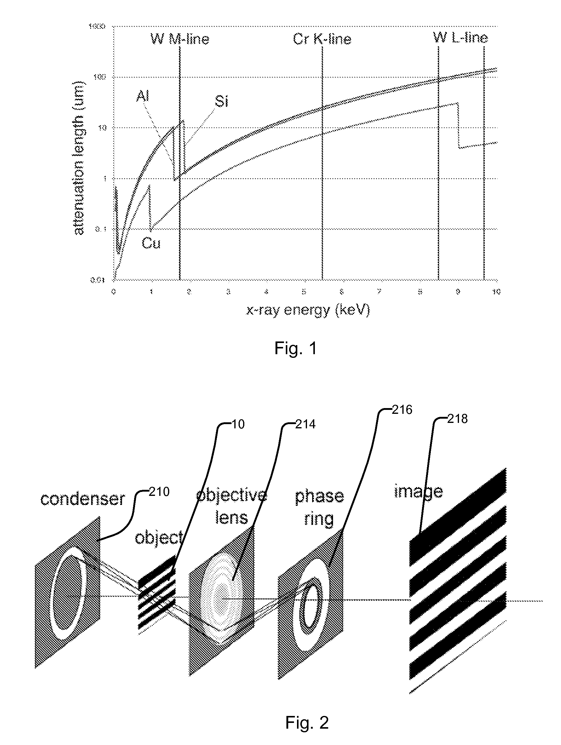
[0022]A number of x-ray imaging systems are disclosed that utilize one or more atomic emission lines to image specific materials in a sample, taking advantage of the spectral absorption properties of the sample to produce high image contrast with appropriate imaging mechanisms. It also takes into account the response of optics and detectors at different x-ray energies. It deals, in particular, with materials used in current generation and next generation semiconductor integrated circuit devices.

[0023]As an example, refer to FIG. 1, which shows the absorption spectrum of materials used most frequently in semiconductor devices: Copper, Aluminum, and Silicon. Typically copper or aluminum circuits are fabricated in a silicon substrate. To image the circuit structure, strong contrast is desirable between the circuit structure and the silicon substrate.

[0024]The interaction of x-rays with most materials is complex and strongly dependent on the x-ray energy. A good example is illustrated i...


PUM


Abstract

An x-ray imaging system uses particular emission lines that are optimized for imaging specific metallic structures in a semiconductor integrated circuit structures and optimized for the use with specific optical elements and scintillator materials. Such a system is distinguished from currently-existing x-ray imaging systems that primarily use the integral of all emission lines and the broad Bremstralung radiation. The disclosed system provides favorable imaging characteristics such as ability to enhance the contrast of certain materials in a sample, to use different contrast mechanisms in a single imaging system, and to increase the throughput of the system.

Description

RELATED APPLICATIONS[0001]This application claims priority to U.S. Provisional Application No. 60 / 518,369, filed Nov. 7, 2003, which is incorporated herein by reference in its entirety.BACKGROUND OF THE INVENTION[0002]X-ray imaging is a valuable technology for non-destructive imaging applications in medicine and industrial research and development.[0003]All x-ray imaging systems include a source that generates the x-ray beam, which is used to probe the object to be examined, and a detector system for collecting the x-ray beam. The x-ray source is typically an electron-bombardment, a laser-plasma, or a synchrotron radiation source. The detector system is typically based on x-ray film or an electronic, such as charge-coupled device (CCD), detector. In some cases, an intervening scintillator is used to convert the x-ray radiation to a wavelength that is detectable by the detector device.[0004]Further, the x-ray beam is often modified by one or more beam-conditioning devices. Sometimes ...

Claims


Application Information

Patent Timeline
Patent Type & Authority Patents(United States)
IPC IPC(8): G21K1/06
CPCG21K1/06G21K7/00G21K2207/005G21K2201/067
Inventor WANG, YUXINYUN, WENBINGDUEWER, FREDERICK WILLIAM
Owner CARL ZEISS X RAY MICROSCOPY
Why Eureka
Try Eureka